SNVSAG3B November 2015 – December 2024 LMR14030-Q1
PRODUCTION DATA
- 1
- 1 Features
- 2 Applications
- 3 Description
- 4 Pin Configuration and Functions
- 5 Specifications
-
6 Detailed Description
- 6.1 Overview
- 6.2 Functional Block Diagram
- 6.3
Feature Description
- 6.3.1 Fixed Frequency Peak Current Mode Control
- 6.3.2 Slope Compensation
- 6.3.3 Sleep-mode
- 6.3.4 Low Dropout Operation and Bootstrap Voltage (BOOT)
- 6.3.5 Adjustable Output Voltage
- 6.3.6 Enable and Adjustable Undervoltage Lockout
- 6.3.7 External Soft-start
- 6.3.8 Switching Frequency and Synchronization (RT/SYNC)
- 6.3.9 Power Good (PGOOD)
- 6.3.10 Over Current and Short Circuit Protection
- 6.3.11 Overvoltage Protection
- 6.3.12 Thermal Shutdown
- 6.4 Device Functional Modes
- 7 Application and Implementation
- 8 Device and Documentation Support
- 9 Revision History
- 10Mechanical, Packaging, and Orderable Information
パッケージ・オプション
メカニカル・データ(パッケージ|ピン)
サーマルパッド・メカニカル・データ
- DDA|8
発注情報
4 Pin Configuration and Functions
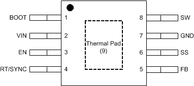
 Figure 4-1 DDA Package8-Pin (HSOIC)Top View
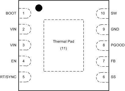
 Figure 4-2 DPR Package10-Pin (WSON)Top View
Table 4-1 Pin Functions
| NAME | NO. | TYPE (1) | DESCRIPTION | |
|---|---|---|---|---|
| SO-8 | WSON-10 | |||
| BOOT | 1 | 1 | P | Bootstrap capacitor connection for high-side MOSFET driver. Connect a high quality 0.1 μF capacitor from BOOT to SW. |
| VIN | 2 | 2, 3 | P | Connect to power supply and bypass capacitors CIN. Path from VIN pin to high frequency bypass CIN and GND must be as short as possible. |
| EN | 3 | 4 | A | Enable pin, with internal pull-up current source. Pull below 1.2V to disable. Float or connect to VIN to enable. Adjust the input under voltage lockout with two resistors. See the Enable and Adjusting Under voltage lockout section. |
| RT/SYNC | 4 | 5 | A | Resistor Timing or External Clock input. An internal amplifier holds this pin at a fixed voltage when using an external resistor to ground to set the switching frequency. If the pin is pulled above the PLL upper threshold, a mode change occurs and the pin becomes a synchronization input. The internal amplifier is disabled and the pin is a high impedance clock input to the internal PLL. If clocking edges stop, the internal amplifier is re-enabled and the operating mode returns to frequency programming by resistor. |
| FB | 5 | 7 | A | Feedback input pin, connect to the feedback divider to set VOUT. Do not short this pin to ground during operation. |
| SS | 6 | 6 | A | Soft-start control pin. Connect to a capacitor to set soft-start time. |
| PGOOD | N/A | 8 | A | Open drain output for power-good flag. Use a 10kΩ to 100kΩ pull-up resistor to logic rail or other DC voltage no higher than 7V. |
| GND | 7 | 9 | G | System ground pin. |
| SW | 8 | 10 | P | Switching output of the regulator. Internally connected to high-side power MOSFET. Connect to power inductor. |
| Thermal Pad | 9 | 11 | G | Major heat dissipation path of the die. Must be connected to ground plane on PCB. |
(1) A = Analog, P = Power, G = Ground