JAJSCQ0B December 2016 – March 2018 LMR23625-Q1
PRODUCTION DATA.
- 1 特長
- 2 アプリケーション
- 3 概要
- 4 改訂履歴
- 5 Device Comparison
- 6 Pin Configuration and Functions
- 7 Specifications
-
8 Detailed Description
- 8.1 Overview
- 8.2 Functional Block Diagram
- 8.3
Feature Description
- 8.3.1 Fixed-Frequency Peak-Current-Mode Control
- 8.3.2 Adjustable Output Voltage
- 8.3.3 EN/SYNC
- 8.3.4 VCC, UVLO
- 8.3.5 Minimum ON-Time, Minimum OFF-Time and Frequency Foldback at Dropout Conditions
- 8.3.6 Power Good (PGOOD)
- 8.3.7 Internal Compensation and CFF
- 8.3.8 Bootstrap Voltage (BOOT)
- 8.3.9 Overcurrent and Short-Circuit Protection
- 8.3.10 Thermal Shutdown
- 8.4 Device Functional Modes
-
9 Application and Implementation
- 9.1 Application Information
- 9.2
Typical Applications
- 9.2.1 Design Requirements
- 9.2.2
Detailed Design Procedure
- 9.2.2.1 Custom Design With WEBENCH® Tools
- 9.2.2.2 Output Voltage Setpoint
- 9.2.2.3 Switching Frequency
- 9.2.2.4 Inductor Selection
- 9.2.2.5 Output Capacitor Selection
- 9.2.2.6 Feed-Forward Capacitor
- 9.2.2.7 Input Capacitor Selection
- 9.2.2.8 Bootstrap Capacitor Selection
- 9.2.2.9 VCC Capacitor Selection
- 9.2.2.10 Undervoltage Lockout Setpoint
- 9.2.3 Application Curves
- 10Power Supply Recommendations
- 11Layout
- 12デバイスおよびドキュメントのサポート
- 13メカニカル、パッケージ、および注文情報
パッケージ・オプション
メカニカル・データ(パッケージ|ピン)
サーマルパッド・メカニカル・データ
発注情報
8.3.1 Fixed-Frequency Peak-Current-Mode Control
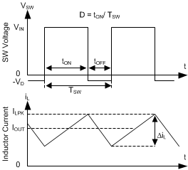
The following operating description of the LMR23625-Q1 refer to the Functional Block Diagram and to the waveforms in Figure 13. LMR23625-Q1 is a step-down synchronous buck regulator with integrated high-side (HS) and low-side (LS) switches (synchronous rectifier). The LMR23625-Q1 supplies a regulated output voltage by turning on the HS and LS NMOS switches with controlled duty cycle. During high-side switch ON time, the SW pin voltage swings up to approximately VIN, and the inductor current iL increase with linear slope (VIN – VOUT) / L. When the HS switch is turned off by the control logic, the LS switch is turned on after an anti-shoot-through dead time. Inductor current discharges through the LS switch with a slope of –VOUT / L. The control parameter of a buck converter is defined as duty cycle D = tON / TSW, where tON is the high-side switch ON time and TSW is the switching period. The regulator control loop maintains a constant output voltage by adjusting the duty cycle D. In an ideal buck converter, where losses are ignored, D is proportional to the output voltage and inversely proportional to the input voltage: D = VOUT / VIN.
 Figure 13. SW Node and Inductor Current Waveforms in
Continuous Conduction Mode (CCM)
The LMR23625-Q1 employs fixed-frequency peak-current-mode control. A voltage feedback loop is used to get accurate DC voltage regulation by adjusting the peak current command based on voltage offset. The peak inductor current is sensed from the high-side switch and compared to the peak current threshold to control the ON-time of the high-side switch. The voltage feedback loop is internally compensated, which allows for fewer external components, makes it easy to design, and provides stable operation with almost any combination of output capacitors. The regulator operates with fixed switching frequency at normal load condition. At light load condition, the LMR23625-Q1 operates in PFM mode to maintain high efficiency (PFM option) or in FPWM mode for low output voltage ripple, tight output voltage regulation, and constant switching frequency (FPWM option).