JAJSCQ0B December 2016 – March 2018 LMR23625-Q1
PRODUCTION DATA.
- 1 特長
- 2 アプリケーション
- 3 概要
- 4 改訂履歴
- 5 Device Comparison
- 6 Pin Configuration and Functions
- 7 Specifications
-
8 Detailed Description
- 8.1 Overview
- 8.2 Functional Block Diagram
- 8.3
Feature Description
- 8.3.1 Fixed-Frequency Peak-Current-Mode Control
- 8.3.2 Adjustable Output Voltage
- 8.3.3 EN/SYNC
- 8.3.4 VCC, UVLO
- 8.3.5 Minimum ON-Time, Minimum OFF-Time and Frequency Foldback at Dropout Conditions
- 8.3.6 Power Good (PGOOD)
- 8.3.7 Internal Compensation and CFF
- 8.3.8 Bootstrap Voltage (BOOT)
- 8.3.9 Overcurrent and Short-Circuit Protection
- 8.3.10 Thermal Shutdown
- 8.4 Device Functional Modes
-
9 Application and Implementation
- 9.1 Application Information
- 9.2
Typical Applications
- 9.2.1 Design Requirements
- 9.2.2
Detailed Design Procedure
- 9.2.2.1 Custom Design With WEBENCH® Tools
- 9.2.2.2 Output Voltage Setpoint
- 9.2.2.3 Switching Frequency
- 9.2.2.4 Inductor Selection
- 9.2.2.5 Output Capacitor Selection
- 9.2.2.6 Feed-Forward Capacitor
- 9.2.2.7 Input Capacitor Selection
- 9.2.2.8 Bootstrap Capacitor Selection
- 9.2.2.9 VCC Capacitor Selection
- 9.2.2.10 Undervoltage Lockout Setpoint
- 9.2.3 Application Curves
- 10Power Supply Recommendations
- 11Layout
- 12デバイスおよびドキュメントのサポート
- 13メカニカル、パッケージ、および注文情報
パッケージ・オプション
メカニカル・データ(パッケージ|ピン)
サーマルパッド・メカニカル・データ
発注情報
8.3.6 Power Good (PGOOD)
The LMR23625AP has a built-in power-good flag shown on PGOOD pin to indicate whether the output voltage is within its regulation level. The PGOOD signal can be used for start-up sequencing of multiple rails or fault protection. The PGOOD pin is an open-drain output that requires a pullup resistor to an appropriate DC voltage. Voltage detected by the PGOOD pin must never exceed 15 V; limit the maximum current into this pin to 1 mA. A resistor divider pair can be used to divide the voltage down from a higher potential. A typical range of pullup resistor value is 10 kΩ to 100 kΩ.
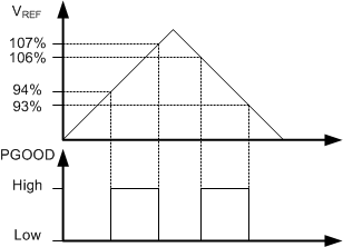
When the FB voltage is within the power-good band, +6% above and –6% below the internal reference VREF typically, the PGOOD switch is turned off, and the PGOOD voltage is pulled up to the voltage level defined by the pullup resistor or divider. When the FB voltage is outside of the tolerance band, +7% above or –7% below VREF typically, the PGOOD switch is turned on, and the PGOOD pin voltage is pulled low to indicate power bad. A glitch filter prevents false-flag operation for short excursions in the output voltage, such as during line and load transients. The values for the various filter and delay times can be found in Typical Characteristics. Power-good operation can best be understood by reference to Figure 20.
 Figure 20. Power-Good Flag