JAJSEU3E February 2018 – November 2020 LMR33620
PRODUCTION DATA
- 1 特長
- 2 アプリケーション
- 3 概要
- 4 Revision History
- 5 Device Comparison Table
- 6 Pin Configuration and Functions
- 7 Specifications
- 8 Detailed Description
-
9 Application and Implementation
- 9.1 Application Information
- 9.2
Typical Application
- 9.2.1 Design Requirements
- 9.2.2
Detailed Design Procedure
- 9.2.2.1 Custom Design With WEBENCH® Tools
- 9.2.2.2 Choosing the Switching Frequency
- 9.2.2.3 Setting the Output Voltage
- 9.2.2.4 Inductor Selection
- 9.2.2.5 Output Capacitor Selection
- 9.2.2.6 Input Capacitor Selection
- 9.2.2.7 CBOOT
- 9.2.2.8 VCC
- 9.2.2.9 CFF Selection
- 9.2.2.10 External UVLO
- 9.2.2.11 Maximum Ambient Temperature
- 9.2.3 Application Curves
- 9.3 What to Do and What Not to Do
- 10Layout
- 11Device and Documentation Support
パッケージ・オプション
デバイスごとのパッケージ図は、PDF版データシートをご参照ください。
メカニカル・データ(パッケージ|ピン)
- RNX|12
- DDA|8
サーマルパッド・メカニカル・データ
発注情報
8.4.2 Dropout
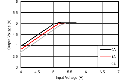
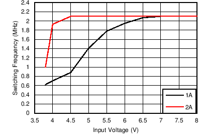
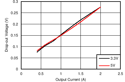
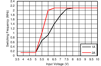
The dropout performance of any buck regulator is affected by the RDSON of the power MOSFETs, the DC resistance of the inductor and the maximum duty cycle that the controller can achieve. As the input voltage level approaches the output voltage, the off-time of the high-side MOSFET starts to approach the minimum value (see Section 7.6). Beyond this point, the switching can become erratic, and the output voltage falls out of regulation. To avoid this problem, the LMR33620 automatically reduces the switching frequency to increase the effective duty cycle and maintain regulation. In this data sheet, the dropout voltage is defined as the difference between the input and output voltage when the output has dropped by 1% of its nominal value. Under this condition, the switching frequency has dropped to its minimum value of about 140 kHz. Note that the 0.4 V short circuit detection threshold is not activated when in dropout mode. Typical dropout characteristics can be found in Figure 8-9, Figure 8-10, Figure 8-11, and Figure 8-12.
 Figure 8-9 Overall Dropout Characteristic VOUT =
5 V
 Figure 8-11 Typical Switching Frequency in Dropout Mode
VOUT = 3.3 V, fSW = 2.1
MHz
 Figure 8-10 Typical Dropout Voltage versus Output Current in
Frequency Foldback ƒSW = 140
kHz
 Figure 8-12 Typical Switching Frequency in Dropout Mode
VOUT = 5 V, fSW = 2.1
MHz