JAJSJN9 January 2021 LMR36015S
PRODUCTION DATA
- 1 特長
- 2 アプリケーション
- 3 概要
- 4 Revision History
- 5 概要 (続き)
- 6 Device Comparison Table
- 7 Pin Configuration and Functions
- 8 Specifications
- 9 Detailed Description
-
10Application and Implementation
- 10.1 Application Information
- 10.2
Typical Application
- 10.2.1
Design 1: Low Power 24-V, 1.5-A PFM Converter
- 10.2.1.1 Design Requirements
- 10.2.1.2
Detailed Design Procedure
- 10.2.1.2.1 Custom Design With WEBENCH Tools
- 10.2.1.2.2 Choosing the Switching Frequency
- 10.2.1.2.3 Setting the Output Voltage
- 10.2.1.2.4 Inductor Selection
- 10.2.1.2.5 Output Capacitor Selection
- 10.2.1.2.6 Input Capacitor Selection
- 10.2.1.2.7 CBOOT
- 10.2.1.2.8 VCC
- 10.2.1.2.9 CFF Selection
- 10.2.1.2.10 Maximum Ambient Temperature
- 10.2.2 Application Curves
- 10.2.3 Design 2: High Density 24-V, 1.5-A FPWM Converter
- 10.2.1
Design 1: Low Power 24-V, 1.5-A PFM Converter
- 10.3 What to Do and What Not to Do
- 11Power Supply Recommendations
- 12Layout
- 13Device and Documentation Support
- 14Mechanical, Packaging, and Orderable Information
9.4.3 Dropout
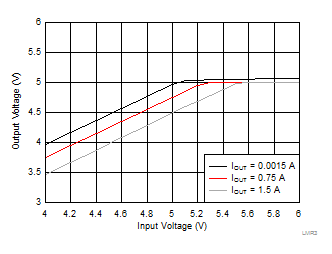
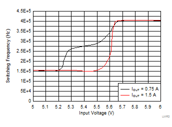
The dropout performance of any buck regulator is affected by the RDSON of the power MOSFETs, the DC resistance of the inductor, and the maximum duty cycle that the controller can achieve. As the input voltage is reduced to near the output voltage, the off-time of the high-side MOSFET starts to approach the minimum value. Beyond this point, the switching can become erratic, the output voltage falls out of regulation, or both. To avoid this problem, the LMR36015S automatically reduces the switching frequency to increase the effective duty cycle and maintain regulation. In this data sheet, the dropout voltage is defined as the difference between the input and output voltage when the output has dropped by 1% of its nominal value. Under this condition, the switching frequency has dropped to its minimum value of about 140 kHz. Note that the 0.4-V short circuit detection threshold is not activated when in dropout mode. Typical dropout characteristics can be found in Figure 9-9 and Figure 9-10.
 Figure 9-9 Overall Dropout Characteristic
 VOUT = 5 V
 Figure 9-10 Frequency Dropout Characteristics ƒSW =
400 kHz