JAJSIO5B July 2019 – February 2020 LMR36506-Q1
ADVANCE INFORMATION for pre-production products; subject to change without notice.
- 1 特長
- 2 アプリケーション
- 3 概要
- 4 改訂履歴
- 5 Device Comparison Table
- 6 Pin Configuration and Functions
- 7 Specifications
-
8 Detailed Description
- 8.1 Overview
- 8.2 Functional Block Diagram
- 8.3
Feature Description
- 8.3.1 Output Voltage Selection
- 8.3.2 Enable and Start-up
- 8.3.3 External CLK SYNC (with MODE/SYNC)
- 8.3.4 Adjustable Switching Frequency (with RT)
- 8.3.5 Power-Good Flag Output
- 8.3.6 Internal LDO, VCC UVLO, and VOUT/BIAS Input
- 8.3.7 Bootstrap Voltage and VCBOOT-UVLO (CBOOT Terminal)
- 8.3.8 Spread Spectrum
- 8.3.9 Soft Start and Recovery from Dropout
- 8.3.10 Current Limit and Short Circuit
- 8.3.11 Thermal Shutdown
- 8.4 Device Functional Modes
-
9 Application and Implementation
- 9.1 Application Information
- 9.2
Typical Application
- 9.2.1 Design Requirements
- 9.2.2 Detailed Design Procedure
- 9.3 What to Do and What Not to Do
- 10Power Supply Recommendations
- 11Layout
- 12デバイスおよびドキュメントのサポート
- 13メカニカル、パッケージ、および注文情報
パッケージ・オプション
メカニカル・データ(パッケージ|ピン)
- RPE|9
サーマルパッド・メカニカル・データ
- RPE|9
発注情報
8.3.10 Current Limit and Short Circuit
The LMR36506-Q1 is protected from overcurrent conditions by cycle-by-cycle current limiting on both high-side and low-side MOSFETs.
High-side MOSFET overcurrent protection is implemented by the typical peak-current mode control scheme. The HS switch current is sensed when the HS is turned on after a short blanking time. The HS switch current is compared to either the minimum of a fixed current set point or the output of the internal error amplifier loop minus the slope compensation every switching cycle. Since the output of the internal error amplifier loop has a maximum value and slope compensation increases with duty cycle, HS current limit decreases with increased duty factor if duty factor is typically above 35%.
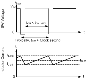
When the LS switch is turned on, the current going through it is also sensed and monitored. Like the high-side device, the low-side device has a turnoff commanded by the internal error amplifier loop. In the case of the low-side device, turnoff is prevented if the current exceeds this value, even if the oscillator normally starts a new switching cycle. Also like the high-side device, there is a limit on how high the turnoff current is allowed to be. This is called the low-side current limit, ILS-LIMIT (or IL-LS in Figure 7). If the LS current limit is exceeded, the LS MOSFET stays on and the HS switch is not be turned on. The LS switch is turned off once the LS current falls below this limit and the HS switch is turned on again as long as at least one clock period has passed since the last time the HS device has turned on.
 Figure 7. Current Limit Waveforms
 The net effect of the operation of high-side and low-side current limit is that the IC operates in hysteretic control. Also, since the current waveform assumes values between ISC (or IL-HS in Figure 7) and ILS-LIMIT, output current is very close to the average of these two values unless duty factor is very high. Once operating in current limit, hysteretic control is used and current does not increase as output voltage approaches zero.
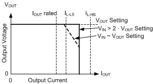
If duty factor is very high, current ripple must be very low in order to prevent instability. Since current ripple is low, the part is able to deliver full current. The current delivered is very close to ILS-LIMIT.
 Figure 8. Output Voltage versus Output Current
 Under most conditions, current is limited to the average of IL-HS and IL-LS, which is approximately 1.4 times the maximum-rated current. If input voltage is low, current can be limited to approximately IL-LS. Also note that current does not exceed the average of IL-HS and IL-LS. Once the overload is removed, the part recovers as though in soft start.