JAJSIO5B July 2019 – February 2020 LMR36506-Q1
ADVANCE INFORMATION for pre-production products; subject to change without notice.
- 1 特長
- 2 アプリケーション
- 3 概要
- 4 改訂履歴
- 5 Device Comparison Table
- 6 Pin Configuration and Functions
- 7 Specifications
-
8 Detailed Description
- 8.1 Overview
- 8.2 Functional Block Diagram
- 8.3
Feature Description
- 8.3.1 Output Voltage Selection
- 8.3.2 Enable and Start-up
- 8.3.3 External CLK SYNC (with MODE/SYNC)
- 8.3.4 Adjustable Switching Frequency (with RT)
- 8.3.5 Power-Good Flag Output
- 8.3.6 Internal LDO, VCC UVLO, and VOUT/BIAS Input
- 8.3.7 Bootstrap Voltage and VCBOOT-UVLO (CBOOT Terminal)
- 8.3.8 Spread Spectrum
- 8.3.9 Soft Start and Recovery from Dropout
- 8.3.10 Current Limit and Short Circuit
- 8.3.11 Thermal Shutdown
- 8.4 Device Functional Modes
-
9 Application and Implementation
- 9.1 Application Information
- 9.2
Typical Application
- 9.2.1 Design Requirements
- 9.2.2 Detailed Design Procedure
- 9.3 What to Do and What Not to Do
- 10Power Supply Recommendations
- 11Layout
- 12デバイスおよびドキュメントのサポート
- 13メカニカル、パッケージ、および注文情報
パッケージ・オプション
メカニカル・データ(パッケージ|ピン)
- RPE|9
サーマルパッド・メカニカル・データ
- RPE|9
発注情報
11.1 Layout Guidelines
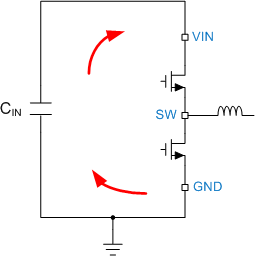
The PCB layout of any DC/DC converter is critical to the optimal performance of the design. Poor PCB layout can disrupt the operation of an otherwise good schematic design. Even if the converter regulates correctly, bad PCB layout can mean the difference between a robust design and one that cannot be mass produced. Furthermore, to a great extent, the EMI performance of the regulator is dependent on the PCB layout. In a buck converter, the most critical PCB feature is the loop formed by the input capacitor or capacitors and power ground, as shown in Figure 11. This loop carries large transient currents that can cause large transient voltages when reacting with the trace inductance. These unwanted transient voltages disrupt the proper operation of the converter. Because of this, the traces in this loop must be wide and short, and the loop area as small as possible to reduce the parasitic inductance. Figure 12 shows a recommended layout for the critical components of the LMR36506-Q1.
- Place the input capacitors as close as possible to the VIN and GND terminals. VIN and GND pins are adjacent, simplifying the input capacitor placement.
- Place bypass capacitor for VCC close to the VCC pin. This capacitor must be placed close to the device and routed with short, wide traces to the VCC and GND pins.
- Use wide traces for the CBOOT capacitor. Place CBOOT close to the device with short/wide traces to the BOOT and SW pins. Route the SW pin to the N/C pin and used to connect the BOOT capacitor to SW.
- Place the feedback divider as close as possible to the FB pin of the device. Place RFBB, RFBT, and CFF, if used, physically close to the device. The connections to FB and GND must be short and close to those pins on the device. The connection to VOUT can be somewhat longer. However, the latter trace must not be routed near any noise source (such as the SW node) that can capacitively couple into the feedback path of the regulator.
- Use at least one ground plane in one of the middle layers. This plane acts as a noise shield and as a heat dissipation path.
- Provide wide paths for VIN, VOUT, and GND. Making these paths as wide and direct as possible reduces any voltage drops on the input or output paths of the converter and maximizes efficiency.
- Provide enough PCB area for proper heat-sinking. As stated in the Maximum Ambient Temperature section, enough copper area must be used to ensure a low RθJA, commensurate with the maximum load current and ambient temperature. The top and bottom PCB layers must be made with two ounce copper and no less than one ounce. If the PCB design uses multiple copper layers (recommended), these thermal vias can also be connected to the inner layer heat-spreading ground planes.
- Keep switch area small. Keep the copper area connecting the SW pin to the inductor as short and wide as possible. At the same time, the total area of this node must be minimized to help reduce radiated EMI.
See the following PCB layout resources for additional important guidelines:
- Layout Guidelines for Switching Power Supplies Application Report
- Simple Switcher PCB Layout Guidelines Application Report
- Construction Your Power Supply- Layout Considerations Seminar
- Low Radiated EMI Layout Made Simple with LM4360x and LM4600x Application Report
 Figure 11. Current Loops with Fast Edges