JAJSME1E August   2021  – September 2023 LMR38020

PRODUCTION DATA  

  1.   1
  2. 特長
  3. アプリケーション
  4. 概要
  5. Revision History
  6. Device Comparison Table
  7. Pin Configuration and Functions
  8. Specifications
    1. 7.1 Absolute Maximum Ratings
    2. 7.2 ESD Ratings
    3. 7.3 Recommended Operating Conditions
    4. 7.4 Thermal Information
    5. 7.5 Electrical Characteristics
    6. 7.6 System Characteristics
    7. 7.7 Typical Characteristics
  9. Detailed Description
    1. 8.1 Overview
    2. 8.2 Functional Block Diagram
    3. 8.3 Feature Description
      1. 8.3.1  Fixed Frequency Peak Current Mode Control
      2. 8.3.2  Adjustable Output Voltage
      3. 8.3.3  Enable
      4. 8.3.4  Switching Frequency and Synchronization (RT/SYNC)
      5. 8.3.5  Power-Good Flag Output
      6. 8.3.6  Minimum On Time, Minimum Off Time, and Frequency Foldback
      7. 8.3.7  Bootstrap Voltage
      8. 8.3.8  Overcurrent and Short Circuit Protection
      9. 8.3.9  Soft Start
      10. 8.3.10 Thermal Shutdown
    4. 8.4 Device Functional Modes
      1. 8.4.1 Auto Mode
      2. 8.4.2 Forced PWM Operation
      3. 8.4.3 Dropout
      4. 8.4.4 Minimum Switch On Time
  10. Application and Implementation
    1. 9.1 Application Information
    2. 9.2 Typical Application
      1. 9.2.1 Design Requirements
      2. 9.2.2 Detailed Design Procedure
        1. 9.2.2.1 Custom Design With WEBENCH® Tools
        2. 9.2.2.2 Choosing the Switching Frequency
        3. 9.2.2.3 FB for Adjustable Output
        4. 9.2.2.4 Inductor Selection
        5. 9.2.2.5 Output Capacitor Selection
        6. 9.2.2.6 Input Capacitor Selection
        7. 9.2.2.7 CBOOT
        8. 9.2.2.8 External UVLO
        9. 9.2.2.9 Maximum Ambient Temperature
      3. 9.2.3 Application Curves
    3. 9.3 Best Design Practices
    4. 9.4 Power Supply Recommendations
    5. 9.5 Layout
      1. 9.5.1 Layout Guidelines
        1. 9.5.1.1 Ground and Thermal Considerations
      2. 9.5.2 Layout Example
  11. 10Device and Documentation Support
    1. 10.1 Device Support
      1. 10.1.1 Development Support
        1. 10.1.1.1 Custom Design With WEBENCH® Tools
      2. 10.1.2 サード・パーティ製品に関する免責事項
    2. 10.2 Documentation Support
      1. 10.2.1 Related Documentation
    3. 10.3 ドキュメントの更新通知を受け取る方法
    4. 10.4 サポート・リソース
    5. 10.5 Trademarks
    6. 10.6 静電気放電に関する注意事項
    7. 10.7 用語集
  12. 11Mechanical, Packaging, and Orderable Information

パッケージ・オプション

メカニカル・データ(パッケージ|ピン)
サーマルパッド・メカニカル・データ
発注情報

Application Curves

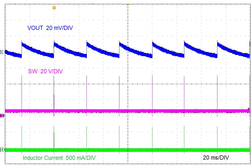
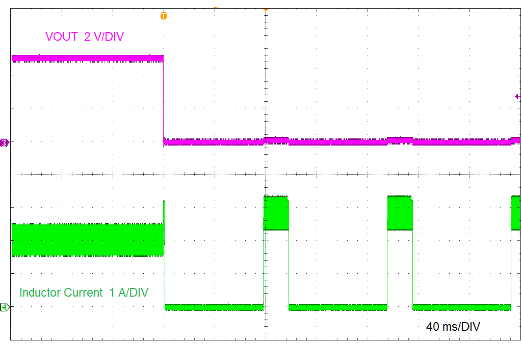
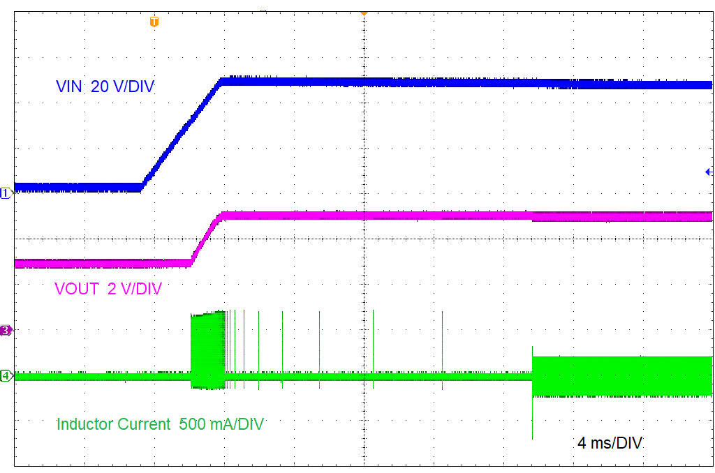
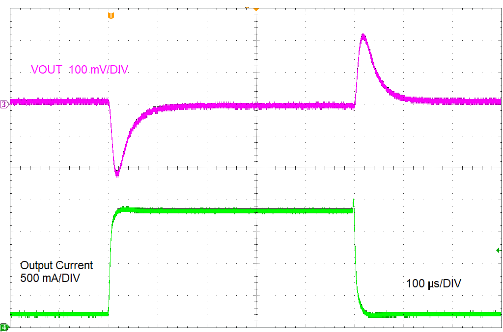
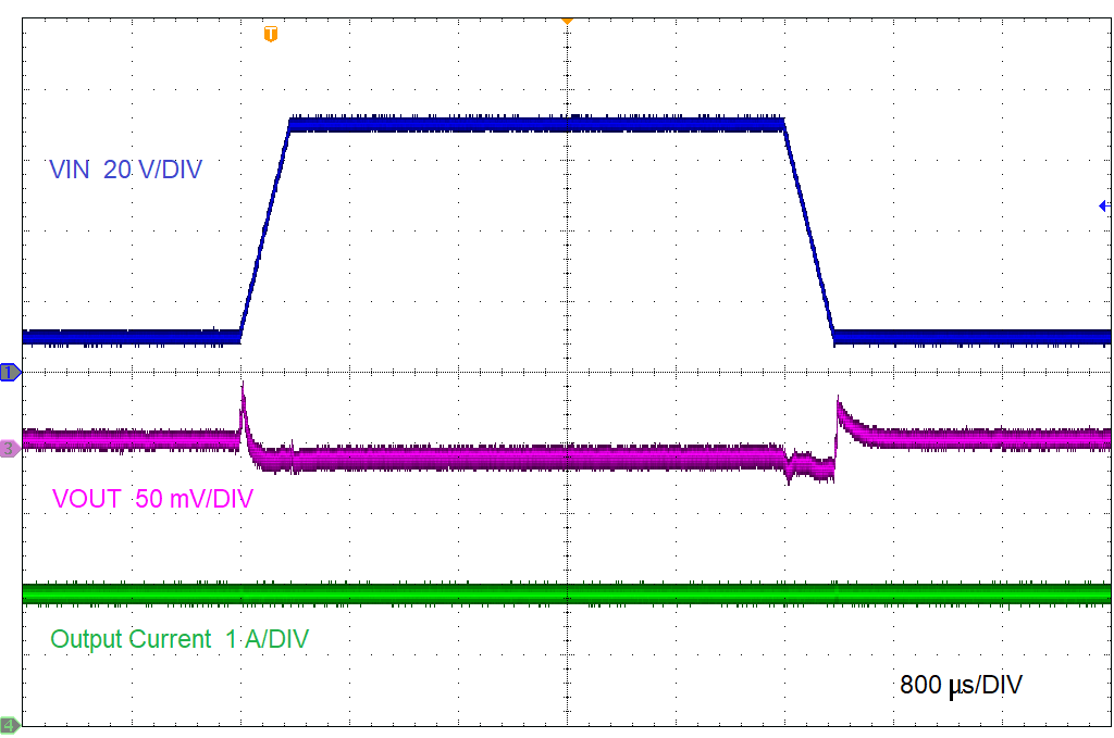
Unless otherwise specified the following conditions apply: VIN = 48 V, L = 15 µH , TA = 25°C.
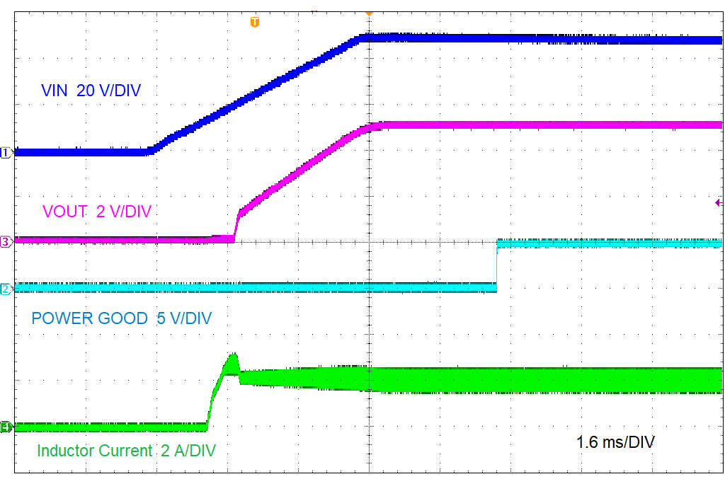
GUID-20211111-SS0I-B5BL-WBGS-H4VTF74J7SGH-low.png
LMR38020VOUT = 5 V400 kHz
Figure 9-3 Start-Up by VIN
GUID-20211112-SS0I-9Q1B-L0HK-SHCHNRNCB188-low.png
LMR38020VOUT = 5 V

AC Coupled

No Load
Figure 9-5 PFM Switching
GUID-20211111-SS0I-VLTN-KBTV-4Q5Q2RPPB05L-low.png
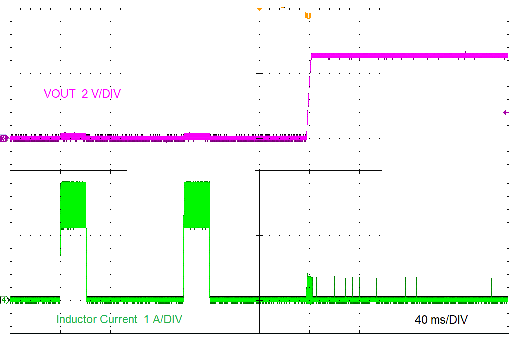
LMR38020VOUT = 5 V2 A to Short
Figure 9-7 Short Circuit Applied
GUID-20211112-SS0I-WV9P-5NPN-QM831BF3KHB3-low.png
LMR38020 FPWMVOUT = 5 V

Bias to 3 V

No Load
Figure 9-9 Start-Up with Prebias
GUID-20211112-SS0I-Z31X-NXNC-CJWVMR25T1ZJ-low.png
LMR38020VOUT = 5 V

(AC Coupled)

400 kHz
200 mA to 1.8 A at 200 mA/µs
Figure 9-11 Load Transient
GUID-20211109-SS0I-M57Z-H0GF-1MGN74CDQ4JP-low.svg
LMR38020VOUT = 5 V

PFM Version

400 kHz
Figure 9-13 5-V Load Regulation
GUID-20211112-SS0I-SX2T-1FGD-MG9PSJ3GXT1Q-low.png
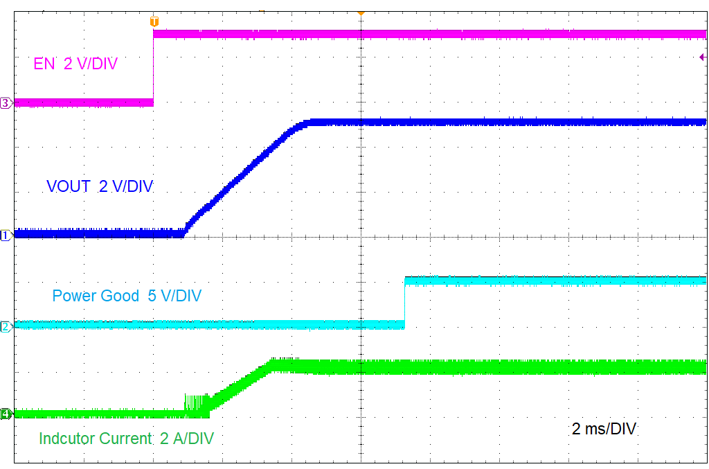
LMR38020VOUT = 5 V400 kHz
Figure 9-4 Start-Up by EN
GUID-20211111-SS0I-2MWJ-CW3J-SPT7NZ3BTJMJ-low.png
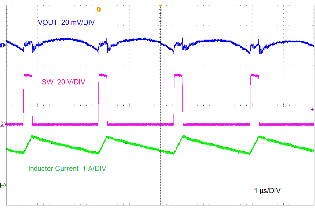
LMR38020VOUT = 5 V

AC Coupled

400 kHz
Figure 9-6 Full Load Switching
GUID-20211112-SS0I-ZFCP-98PG-WX2CWZLPJJV7-low.png
LMR38020VOUT = 5 VShort Recovery
Figure 9-8 Short-Circuit Recovery
GUID-20211112-SS0I-VK3K-SH8T-QTFB2VX8DZR3-low.png
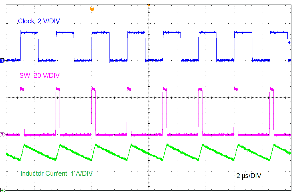
LMR38020VOUT = 5 V400 kHz
Figure 9-10 Frequency Synchronization
GUID-20211115-SS0I-WQDW-DL1C-FZXN5GTF42P7-low.png
LMR38020VOUT = 5 V

(AC Coupled)

400 kHz
10 V to 70 V at 200 V/ms
Figure 9-12 Line Transient
GUID-20211109-SS0I-QVZB-XSHB-QDJRNRRTLWWM-low.svg
LMR38020VOUT = 12 V

PFM Version

400 kHz
Figure 9-14 12-V Load Regulation