JAJSME1E August 2021 – September 2023 LMR38020
PRODUCTION DATA
- 1
- 1 特長
- 2 アプリケーション
- 3 概要
- 4 Revision History
- 5 Device Comparison Table
- 6 Pin Configuration and Functions
- 7 Specifications
-
8 Detailed Description
- 8.1 Overview
- 8.2 Functional Block Diagram
- 8.3
Feature Description
- 8.3.1 Fixed Frequency Peak Current Mode Control
- 8.3.2 Adjustable Output Voltage
- 8.3.3 Enable
- 8.3.4 Switching Frequency and Synchronization (RT/SYNC)
- 8.3.5 Power-Good Flag Output
- 8.3.6 Minimum On Time, Minimum Off Time, and Frequency Foldback
- 8.3.7 Bootstrap Voltage
- 8.3.8 Overcurrent and Short Circuit Protection
- 8.3.9 Soft Start
- 8.3.10 Thermal Shutdown
- 8.4 Device Functional Modes
- 9 Application and Implementation
- 10Device and Documentation Support
- 11Mechanical, Packaging, and Orderable Information
6 Pin Configuration and Functions
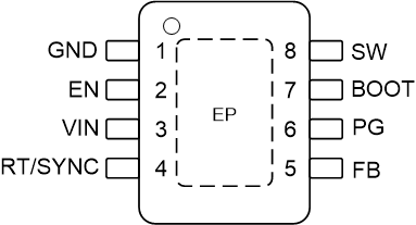
 Figure 6-1 DDA
Package,
8-Pin HSOIC(Top View)
Figure 6-1 DDA
Package,
8-Pin HSOIC(Top View)Table 6-1 Pin Functions
| PIN | TYPE | DESCRIPTION | |
|---|---|---|---|
| NAME | NO. | ||
| GND | 1 | G | Power and analog ground terminal. All electrical parameters are measured with respect to this pin. Connect a high-quality bypass capacitor directly to this pin and VIN with short and wide traces. |
| EN | 2 | A | Enable input to regulator. High = ON, low = OFF. Can be connected directly to VIN. Do not float. |
| VIN | 3 | P | Input supply to the regulator. Connect a high-quality bypass capacitor or capacitors directly to this pin and GND with short and wide traces. |
| RT/SYNC | 4 | A | Resistor timing or external clock input. An internal amplifier holds this pin at a fixed voltage when using an external resistor to ground to set the switching frequency. If the pin is pulled above the PLL upper threshold, a mode change occurs and the pin becomes a synchronization input. The internal amplifier is disabled and the pin is a high impedance clock input to the internal PLL. If clocking edges stop, the internal amplifier is re-enabled and the operating mode returns to frequency programming by resistor. |
| FB | 5 | A | Feedback input to the regulator. Connect to tap point of the feedback voltage divider. Do not float. Do not ground. |
| PG | 6 | A | Open-drain power-good flag output. Connect to a suitable voltage supply through a current limiting resistor. High = power OK, low = power bad. The flag pulls low when EN = low. Can be left open when not used. |
| BOOT | 7 | P | Bootstrap supply voltage for the internal high-side driver. Connect a high-quality 100-nF capacitor from this pin to the SW pin. |
| SW | 8 | P | Regulator switch node. Connect to a power inductor. |
| EP | THERMAL PAD | Thermal | Connect to system ground. |