JAJSN60B december   2020  – may 2023 LMR43610 , LMR43620

PRODUCTION DATA  

  1.   1
  2. 特長
  3. アプリケーション
  4. 概要
  5. Revision History
  6. Device Comparison Table
  7. Pin Configuration and Functions
  8. Specifications
    1. 7.1 Absolute Maximum Ratings
    2. 7.2 ESD Ratings
    3. 7.3 Recommended Operating Conditions
    4. 7.4 Thermal Information
    5. 7.5 Electrical Characteristics
    6. 7.6 System Characteristics
    7. 7.7 Typical Characteristics
  9. Detailed Description
    1. 8.1 Overview
    2. 8.2 Functional Block Diagram
    3. 8.3 Feature Description
      1. 8.3.1  Enable, Start-Up, and Shutdown
      2. 8.3.2  External CLK SYNC (with MODE/SYNC)
        1. 8.3.2.1 Pulse-Dependent MODE/SYNC Pin Control
      3. 8.3.3  Adjustable Switching Frequency (with RT)
      4. 8.3.4  Power-Good Output Operation
      5. 8.3.5  Internal LDO, VCC, and VOUT/FB Input
      6. 8.3.6  Bootstrap Voltage and VBOOT-UVLO (BOOT Terminal)
      7. 8.3.7  Output Voltage Selection
      8. 8.3.8  Soft Start and Recovery from Dropout
        1. 8.3.8.1 Recovery from Dropout
      9. 8.3.9  Current Limit and Short Circuit
      10. 8.3.10 Thermal Shutdown
      11. 8.3.11 Input Supply Current
    4. 8.4 Device Functional Modes
      1. 8.4.1 Shutdown Mode
      2. 8.4.2 Standby Mode
      3. 8.4.3 Active Mode
        1. 8.4.3.1 CCM Mode
        2. 8.4.3.2 Auto Mode – Light-Load Operation
          1. 8.4.3.2.1 Diode Emulation
          2. 8.4.3.2.2 Frequency Reduction
        3. 8.4.3.3 FPWM Mode – Light-Load Operation
        4. 8.4.3.4 Minimum On-Time (High Input Voltage) Operation
        5. 8.4.3.5 Dropout
  10. Application and Implementation
    1. 9.1 Application Information
    2. 9.2 Typical Application
      1. 9.2.1 Design Requirements
      2. 9.2.2 Detailed Design Procedure
        1. 9.2.2.1 Choosing the Switching Frequency
        2. 9.2.2.2 Setting the Output Voltage
          1. 9.2.2.2.1 FB for Adjustable Output
        3. 9.2.2.3 Inductor Selection
        4. 9.2.2.4 Output Capacitor Selection
        5. 9.2.2.5 Input Capacitor Selection
        6. 9.2.2.6 CBOOT
        7. 9.2.2.7 VCC
        8. 9.2.2.8 CFF Selection
          1. 9.2.2.8.1 External UVLO
        9. 9.2.2.9 Maximum Ambient Temperature
      3. 9.2.3 Application Curves
    3. 9.3 Best Design Practices
    4. 9.4 Power Supply Recommendations
    5. 9.5 Layout
      1. 9.5.1 Layout Guidelines
        1. 9.5.1.1 Ground and Thermal Considerations
      2. 9.5.2 Layout Example
  11. 10Device and Documentation Support
    1. 10.1 Device Support
      1. 10.1.1 サード・パーティ製品に関する免責事項
      2. 10.1.2 Device Nomenclature
    2. 10.2 Documentation Support
      1. 10.2.1 Related Documentation
    3. 10.3 サポート・リソース
    4. 10.4 Trademarks
    5. 10.5 静電気放電に関する注意事項
    6. 10.6 用語集
  12. 11Mechanical, Packaging, and Orderable Information

パッケージ・オプション

メカニカル・データ(パッケージ|ピン)
サーマルパッド・メカニカル・データ
発注情報

FPWM Mode – Light-Load Operation

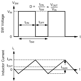
In FPWM mode, frequency is maintained while lightly loaded. To maintain frequency, a limited reverse current is allowed to flow through the inductor. Reverse current is limited by reverse current limit circuitry, see Electrical Characteristics for reverse current limit values.
GUID-E9B1E5D0-BD95-4C66-B137-D5F35089F470-low.gif
In FPWM mode, Continuous Conduction (CCM) is possible even if IOUT is less than half of Iripple.
Figure 8-18 FPWM Mode Operation

For all devices, in FPWM mode, frequency reduction is still available if output voltage is high enough to command minimum on time even while lightly loaded, allowing good behavior during faults which involve output being pulled up.