JAJSSS1 May 2024 LMR51406 , LMR51410
PRODUCTION DATA
- 1
- 1 特長
- 2 アプリケーション
- 3 概要
- 4 Device Comparison Table
- 5 Pin Configuration and Functions
- 6 Specifications
- 7 Detailed Description
-
8 Application and Implementation
- 8.1 Application Information
- 8.2
Typical Application
- 8.2.1 Design Requirements
- 8.2.2
Detailed Design Procedure
- 8.2.2.1 Custom Design With WEBENCH® Tools
- 8.2.2.2 Output Voltage Setpoint
- 8.2.2.3 Switching Frequency
- 8.2.2.4 Inductor Selection
- 8.2.2.5 Output Capacitor Selection
- 8.2.2.6 Input Capacitor Selection
- 8.2.2.7 Bootstrap Capacitor
- 8.2.2.8 Undervoltage Lockout Setpoint
- 8.2.2.9 Replacing Non Sync Buck Converter
- 8.2.3 Application Curves
- 8.3 Power Supply Recommendations
- 8.4 Layout
- 9 Device and Documentation Support
- 10Revision History
- 11Mechanical, Packaging, and Orderable Information
8.2 Typical Application
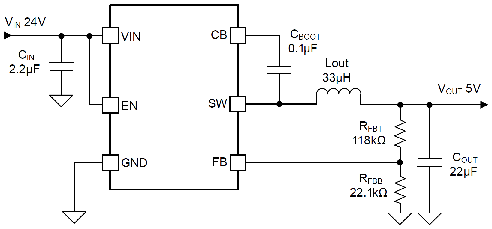
The LMR51410 only requires a few external components to convert from a wide voltage range supply to a fixed output voltage. Figure 8-1 shows a basic schematic.
 Figure 8-1 Application Circuit
The external components have to fulfill the needs of the application and the stability criteria of the control loop of the device. can be used to simplify the output filter component selection.
Table 8-1 L and COUT Typical Values
| fSW (kHz) | VOUT (V) | IOUT (A) | L (µH) | COUT (1) | RFBT (kΩ) | RFBB (kΩ) |
|---|---|---|---|---|---|---|
| 400 | 3.3 | 1 | 22 | 22µF / 10V | 69.8 | 22.1 |
| 5 | 1 | 33 | 22µF / 16V | 118 | 22.1 | |
| 12 | 1 | 56 | 2 × 22µF / 35V | 309 | 22.1 | |
| 1100 | 3.3 | 1 | 8.2 | 10µF / 10V | 69.8 | 22.1 |
| 5 | 1 | 10 | 10µF / 16V | 118 | 22.1 | |
| 12 | 1 | 22 | 22µF + 10µF / 35V | 309 | 22.1 |
(1) Ceramic capacitor is used in this table.