JAJSKO0C October 2021 – November 2022 LMR51420
PRODUCTION DATA
- 1 特長
- 2 アプリケーション
- 3 概要
- 4 Revision History
- 5 Device Comparison Table
- 6 Pin Configuration and Functions
- 7 Specifications
- 8 Detailed Description
- 9 Application and Implementation
- 10Device and Documentation Support
- 11Mechanical, Packaging, and Orderable Information
8.3.1 Fixed Frequency Peak Current Mode Control
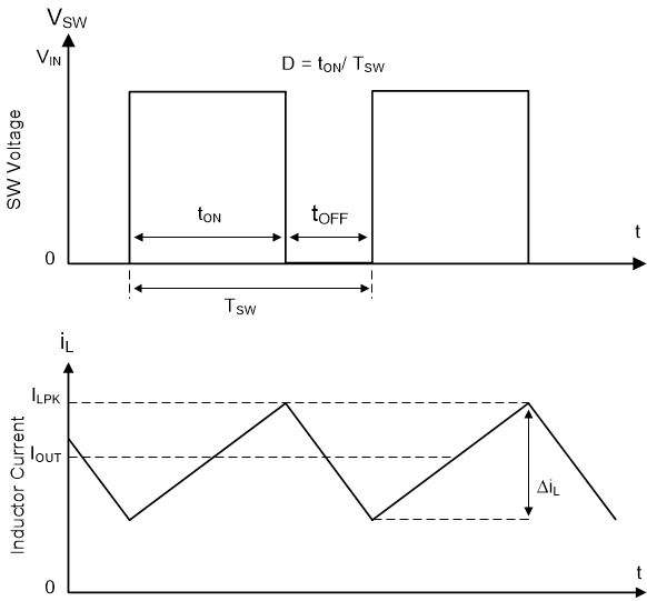
The following operating description of the LMR51420 refers to Section 8.2 and to the waveforms in Figure 8-1. The LMR51420 is a step-down synchronous buck converter with integrated high-side (HS) and low-side (LS) switches (synchronous rectifier). The LMR51420 supplies a regulated output voltage by turning on the high-side and low-side NMOS switches with controlled duty cycle. During the high-side switch on time, the SW pin voltage swings up to approximately VIN, and the inductor current, iL, increases with a linear slope of (VIN – VOUT) / L. When the high-side switch is turned off by the control logic, the low-side switch is turned on after an anti-shoot–through dead time. Inductor current discharges through the low-side switch with a slope of –VOUT / L. The control parameter of a buck converter is defined as:
where
- tON is the high-side switch on time.
- tSW is the switching period.
The converter control loop maintains a constant output voltage by adjusting the duty cycle D. In an ideal buck converter where losses are ignored, and D is proportional to the output voltage and inversely proportional to the input voltage:
 Figure 8-1 SW Node and Inductor Current Waveforms in Continuous Conduction Mode (CCM)
The LMR51420 employs fixed-frequency peak-current mode control. A voltage feedback loop is used to get accurate DC voltage regulation by adjusting the peak-current command based on voltage offset. The peak inductor current is sensed from the high-side switch and compared to the peak current threshold to control the on time of the high-side switch. The voltage feedback loop is internally compensated, which allows for fewer external components, making designing easy and providing stable operation when using a variety of output capacitors. The converter operates with fixed switching frequency at normal load conditions. During light-load condition, the LMR51420 operates in PFM mode to maintain high efficiency (PFM version) or in FPWM mode for low output voltage ripple, tight output voltage regulation, and constant switching frequency (FPWM version).