JAJSPD7 December   2022 LMR51440 , LMR51450

PRODUCTION DATA  

  1. 特長
  2. アプリケーション
  3. 概要
  4. Revision History
  5. Device Comparison Table
  6. Pin Configuration and Functions
  7. Specifications
    1. 7.1 Absolute Maximum Ratings
    2.     ESD Ratings
    3. 7.2 Recommended Operating Conditions
    4. 7.3 Thermal Information
    5. 7.4 Electrical Characteristics
    6. 7.5 System Characteristics
    7. 7.6 Typical Characteristics
  8. Detailed Description
    1. 8.1 Overview
    2. 8.2 Functional Block Diagram
    3. 8.3 Feature Description
      1. 8.3.1  Fixed Frequency Peak Current Mode Control
      2. 8.3.2  Adjustable Output Voltage
      3. 8.3.3  Enable
      4. 8.3.4  Switching Frequency
      5. 8.3.5  Power-Good Flag Output
      6. 8.3.6  Minimum ON-Time, Minimum OFF-Time, and Frequency Foldback
      7. 8.3.7  Bootstrap Voltage
      8. 8.3.8  Overcurrent and Short-Circuit Protection
      9. 8.3.9  Soft Start
      10. 8.3.10 Thermal Shutdown
    4. 8.4 Device Functional Modes
      1. 8.4.1 Shutdown Mode
      2. 8.4.2 Active Mode
      3. 8.4.3 CCM Mode
      4. 8.4.4 Light-Load Operation (PFM Version)
      5. 8.4.5 Light-Load Operation (FPWM Version)
  9. Application and Implementation
    1. 9.1 Application Information
    2. 9.2 Typical Application
      1. 9.2.1 Design Requirements
      2. 9.2.2 Detailed Design Procedure
        1. 9.2.2.1 Output Voltage Set-Point
        2. 9.2.2.2 Switching Frequency
        3. 9.2.2.3 Inductor Selection
        4. 9.2.2.4 Output Capacitor Selection
        5. 9.2.2.5 Input Capacitor Selection
        6. 9.2.2.6 Bootstrap Capacitor
        7. 9.2.2.7 Undervoltage Lockout Set-Point
      3. 9.2.3 Application Curves
    3. 9.3 Best Design Practices
    4. 9.4 Power Supply Recommendations
    5. 9.5 Layout
      1. 9.5.1 Layout Guidelines
        1. 9.5.1.1 Compact Layout for EMI Reduction
        2. 9.5.1.2 Feedback Resistors
      2. 9.5.2 Layout Example
  10. 10Device and Documentation Support
    1. 10.1 Device Support
      1. 10.1.1 Development Support
        1. 10.1.1.1 Custom Design With WEBENCH® Tools
    2. 10.2 Documentation Support
      1. 10.2.1 Related Documentation
    3. 10.3 Receiving Notification of Documentation Updates
    4. 10.4 サポート・リソース
    5. 10.5 Trademarks
    6. 10.6 Electrostatic Discharge Caution
    7. 10.7 Glossary
  11. 11Mechanical, Packaging, and Orderable Information

パッケージ・オプション

メカニカル・データ(パッケージ|ピン)
サーマルパッド・メカニカル・データ
発注情報

Typical Characteristics

VIN = 12 V, fSW= 500 kHz ,TA = 25°C, unless otherwise specified.

fSW = 500 kHzVOUT = 5 VLMR51450
Figure 7-1 5-V Efficiency versus Load Current
fSW = 500 kHzVOUT = 3.3 VLMR51450
Figure 7-3 3.3-V Efficiency versus Load Current
fSW = 500 kHzVOUT = 3.3 VPFM version
Figure 7-5 3.3-V Load Regulation
fSW = 500 kHzVOUT = 5 VPFM version
Figure 7-7 5-V Dropout
GUID-20221118-SS0I-FHXF-N7GW-FCDZZ1R3GNDJ-low.png

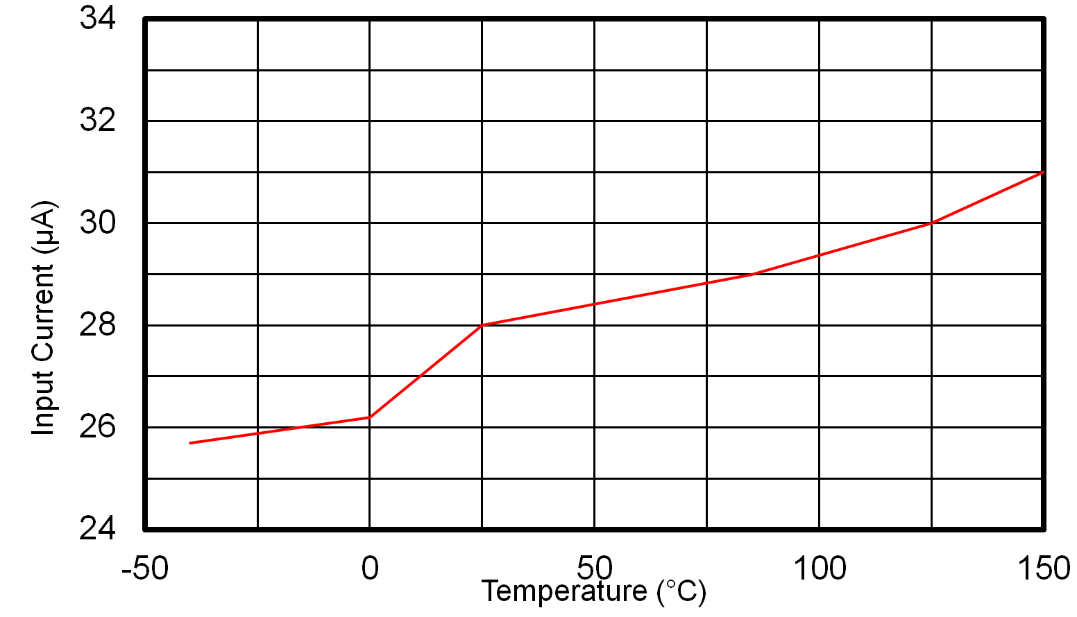
VFB = 1 V

Figure 7-9 Non-Switching Input Supply Current
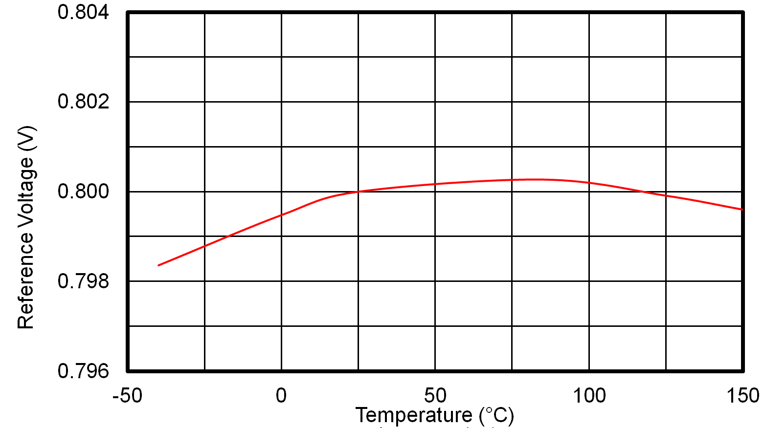
GUID-20221118-SS0I-XL7V-9XRD-QFQTTR6TW2TT-low.pngFigure 7-11 Reference Voltage
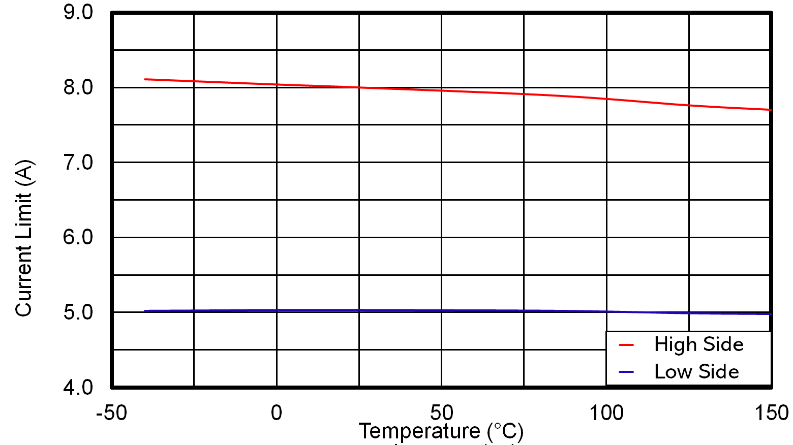
GUID-20221118-SS0I-C80G-FVSD-ZB911X4GLTW5-low.pngFigure 7-13 LMR51450 High Side and Low Side Current Limits
fSW = 500 kHzVOUT = 5 VLMR51440
Figure 7-2 5-V Efficiency versus Load Current
fSW = 500 kHzVOUT = 3.3 VLMR51440
Figure 7-4 3.3-V Efficiency versus Load Current
fSW = 500 kHzVOUT = 5 VPFM version
Figure 7-6 5-V Load Regulation
fSW = 500 kHzVOUT = 3.3 VPFM version
Figure 7-8 3.3-V Dropout
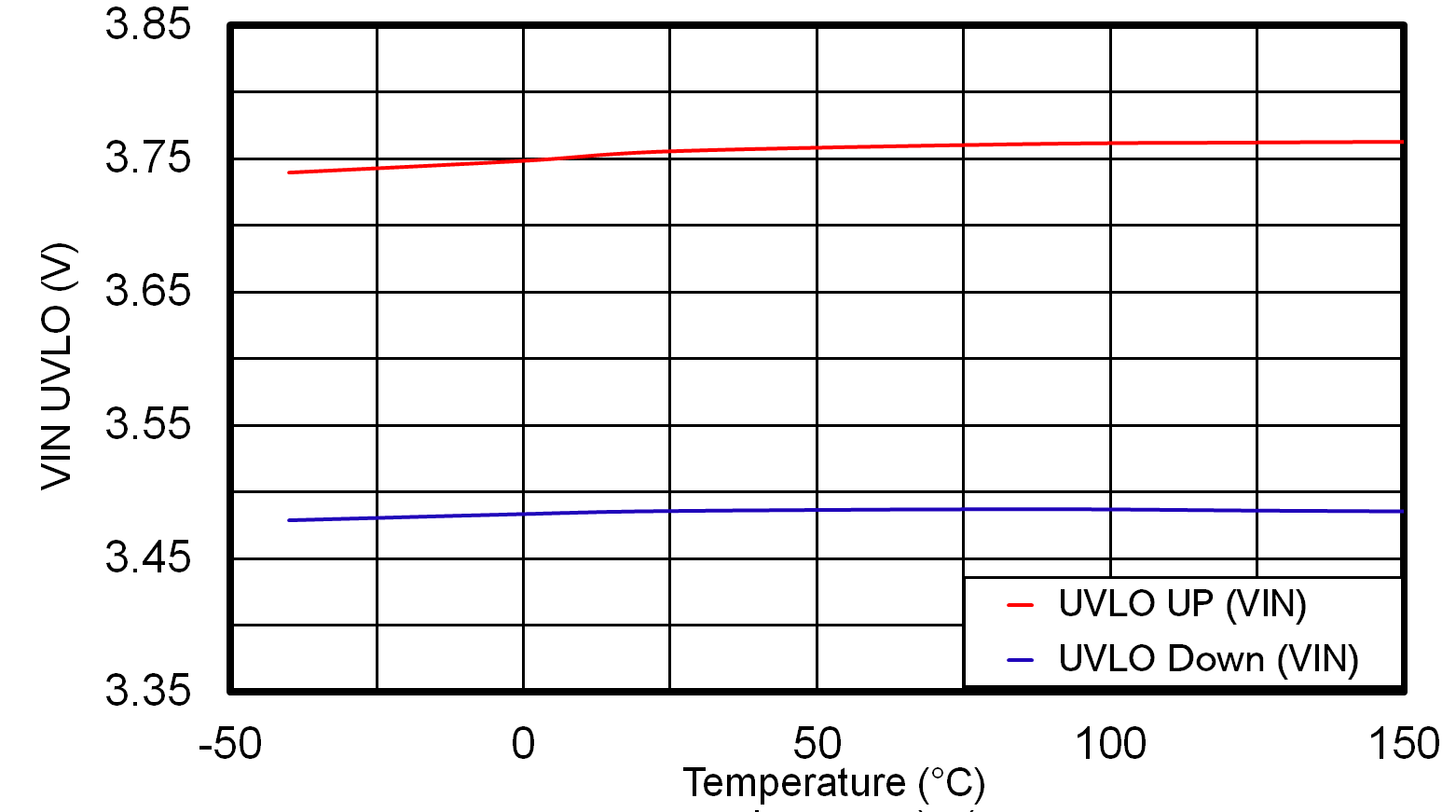
GUID-20221117-SS0I-8NR7-WDRG-MRVB3FWXV8W2-low.png
Figure 7-10 VIN UVLO
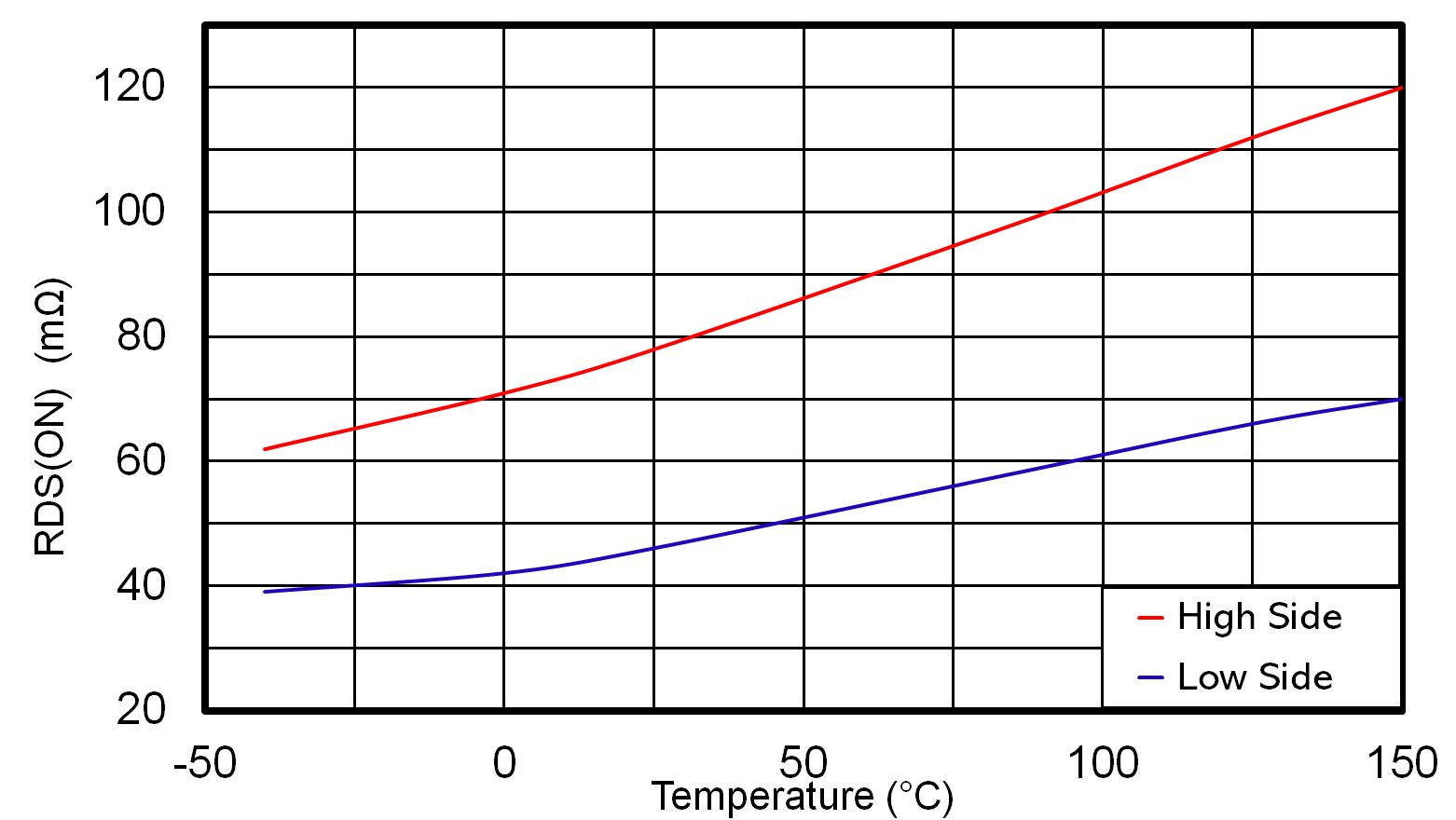
GUID-20221117-SS0I-0G9P-JJ7R-VNC4WZ1KVJ7K-low.pngFigure 7-12 High Side and Low Side Switches RDS_ON
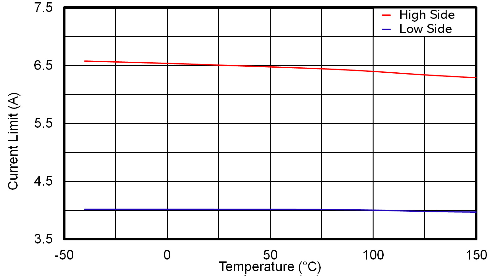
GUID-20221118-SS0I-SXXM-VGBZ-JWJVV5ZGJ6H3-low.pngFigure 7-14 LMR51440 High Side and Low Side Current Limits