SNIS187A March   2015  – July 2015 LMT70 , LMT70A

PRODUCTION DATA.  

  1. Features
  2. Applications
  3. Description
  4. Wide-Range Precision Active RTD or NTC Replacement (−55°C to 150°C)
  5. Revision History
  6. Device Comparison Table
  7. Pin Configuration and Functions
  8. Specifications
    1. 8.1 Absolute Maximum Ratings
    2. 8.2 ESD Ratings
    3. 8.3 Recommended Operating Conditions
    4. 8.4 Thermal Information
    5. 8.5 Electrical Characteristics
    6. 8.6 Electrical Characteristics Temperature Lookup Table (LUT)
    7. 8.7 Switching Characteristics
    8. 8.8 Typical Performance Characteristics
  9. Detailed Description
    1. 9.1 Overview
    2. 9.2 Functional Block Diagram
    3. 9.3 Feature Description
      1. 9.3.1 Temperature Analog Output (TAO)
        1. 9.3.1.1 LMT70 Output Transfer Function
          1. 9.3.1.1.1 First Order Transfer Function
          2. 9.3.1.1.2 Second Order Transfer Function
          3. 9.3.1.1.3 Third Order Transfer Function
        2. 9.3.1.2 LMT70A TAO Matching
        3. 9.3.1.3 TAO Noise Considerations
        4. 9.3.1.4 TAO Capacitive Loads
      2. 9.3.2 TON Digital Input
      3. 9.3.3 Light Sensitivity
    4. 9.4 Device Functional Modes
  10. 10Application and Implementation
    1. 10.1 Application Information
    2. 10.2 Typical Application
      1. 10.2.1 Design Requirements
      2. 10.2.2 Detailed Design Procedure
        1. 10.2.2.1 Temperature Algorithm Selection
        2. 10.2.2.2 ADC Requirements
      3. 10.2.3 Finer Resolution LUT
      4. 10.2.4 Application Curves
    3. 10.3 System Examples
  11. 11Power Supply Recommendations
  12. 12Layout
    1. 12.1 Layout Guidelines
      1. 12.1.1 Mounting and Temperature Conductivity
    2. 12.2 Layout Example
  13. 13Device and Documentation Support
    1. 13.1 Related Links
    2. 13.2 Documentation Support
      1. 13.2.1 Related Documentation
    3. 13.3 Community Resources
    4. 13.4 Trademarks
    5. 13.5 Electrostatic Discharge Caution
    6. 13.6 Glossary
  14. 14Mechanical, Packaging, and Orderable Information

パッケージ・オプション

メカニカル・データ(パッケージ|ピン)
サーマルパッド・メカニカル・データ
発注情報

8 Specifications

8.1 Absolute Maximum Ratings(1)(2)

MIN MAX UNIT
Supply voltage −0.3 6 V
Voltage at T_ON and TAO −0.3 6 V
Current at any pin 5 mA
Storage temperature, Tstg -65 150 °C
(1) Stresses beyond those listed under Absolute Maximum Ratings may cause permanent damage to the device. These are stress ratings only, which do not imply functional operation of the device at these or any other conditions beyond those indicated under Recommended Operating Conditions. Exposure to absolute-maximum-rated conditions for extended periods may affect device reliability.
(2) Soldering process must comply with Reflow Temperature Profile specifications. Refer to www.ti.com/packaging.

8.2 ESD Ratings

VALUE UNIT
V(ESD) Electrostatic discharge Human-body model (HBM), per ANSI/ESDA/JEDEC JS-001(1) ±2000 V
Charged-device model (CDM), per JEDEC specification JESD22-C101(2) ±750
(1) JEDEC document JEP155 states that 500-V HBM allows safe manufacturing with a standard ESD control process.
(2) JEDEC document JEP157 states that 250-V CDM allows safe manufacturing with a standard ESD control process.

8.3 Recommended Operating Conditions

MIN NOM MAX UNIT
Specified temperature (TMIN ≤ TA ≤ TMAX) −55 150 °C
Supply voltage 2.0 5.5 V

8.4 Thermal Information

THERMAL METRIC(1) LMT70 UNIT
DSBGA or WLCSP
YFQ 4 PINS
RθJA Junction-to-ambient thermal resistance 187 °C/W
RθJC(top) Junction-to-case (top) thermal resistance 2.3
RθJB Junction-to-board thermal resistance 105
ψJT Junction-to-top characterization parameter 10.9
ψJB Junction-to-board characterization parameter 104
Thermal response time to 63% of final value in stirred oil (dominated by PCB see layout) 1.5 sec
Thermal response time to 63% of final value in still air (dominated by PCB see layout) 73 sec
(1) For more information about traditional and new thermal metrics, see the IC Package Thermal Metrics application report, SPRA953.

8.5 Electrical Characteristics

Limits apply for TA = TJ = TMIN to TMAX and VDD of 2.00V to 5.5V and VDD ≥ VTAO + 1V, unless otherwise noted.
PARAMETER TEST CONDITIONS MIN TYP MAX UNIT
TEMPERATURE ACCURACY
TAO accuracy
(These stated accuracy limits are with reference to the values in Electrical Characteristics Temperature Lookup Table (LUT), LMT70 temperature-to-voltage.)(1)
TA = –55°C VDD = 2.7 V -0.33 0.33 °C
TA = –40°C VDD = 2.7 V –0.27 0.27
TA = –20°C VDD = 2.7 V –0.2 0.2
TA = –10°C VDD = 2.7 V –0.18 0.18
TA = 20°C to 42°C VDD = 2.7 V –0.13 ±0.05 0.13
TA = 50°C VDD = 2.7 V -0.15 0.15
TA = 90°C VDD = 2.7 V –0.20 0.20
TA = 110°C VDD = 2.7 V –0.23 0.23
TA = 150°C VDD = 2.7 V –0.36 0.36
ATC Accuracy temperature coefficient (note, uses end point calculations)(2) VDD = 2.7V -2.6 +2.6 m°C/°C
APSS Accuracy power supply sensitivity (note uses end point calculations) –55°C ≤ TA ≤ 10°C VDD = VTAO + 1.1 V to 4.0 V –9 –2 8 m°C /V
10°C ≤ TA ≤ 120°C VDD = 2.0 V to 4.0 V
120°C ≤ TA ≤ 150°C VDD = 2.0 V to 4.0 V –15 8
VDD = 4 V to 5.5 V –30 –12 0
VTAO Output Voltage TA = 30°C VDD = 2.7 V 943.227 mV
Sensor gain –5.194 mV/°C
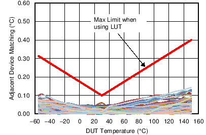
Matching of two adjacent parts in tape and reel for LMT70AYFQR, LMT70AYFQT only (see curve Figure 19 for specification at other temperatures)(3)(2) TA approximately 30°C VDD = 2.0 V to 3.6 V 0.1 °C
TA = 30°C to 150°C 2.5 m°C /°C
TA = 20°C to 30°C VDD = 2.0 V to 3.6 V -2.5
TA = -55°C to 30°C VDD = 2.7 V to 3.6 V –2.5
Time stability(4) 10k hours at 90°C –0.1 ±0.01 0.1 °C
ANALOG OUTPUT
Operating output voltage change with load current 0 µA≤IL≤5 µA 0 0.4 mV
-5 µA≤IL≤0 µA -0.4 0 mV
ROUT Output Resistance 28 80 Ω
TAO Off Leakage Current VTAO ≤ VDD – 0.6v, VT_ON=GND 0.005 0.5 µA
VTAO ≥ 0.2V, VT_ON = GND -0.5 -0.005
Output Load Capacitance 1100 pF
POWER SUPPLY
VDO Dropout Voltage (VDD-VTAO)(5) –20°C ≤ TA ≤ 20°C 1.0  V
–55°C ≤ TA ≤ –20°C 1.1
Power Supply Current 9.2 12 µA
Shutdown Current VDD ≤ 0.4V (-55°C to +110°C) 50 nA
VDD ≤ 0.4V (+110°C to +150°C) 350 nA
LOGIC INPUT
T_ON Logic Low Input Threshold -55°C to +150°C 0.5 0.33*VDD V
T_ON Logic High Input Threshold -55°C to +150°C 0.66*VDD VDD-0.5 V
T_ON Input Current VT_ON = VDD 0.15 1 µA
VT_ON = GND -1 -0.02
(1) Accuracy is defined as the error between the measured and reference output voltages, tabulated in the Conversion Table at the specified conditions of supply voltage and temperature (expressed in °C). These stated accuracy limits are with reference to the values in Electrical Characteristics Temperature Lookup Table (LUT), see Accuracy Curve for other temperatures. Accuracy limits do not include load regulation or aging; they assume no DC load.
(2) The accuracy temperature coefficient specification is given to indicate part to part performance and does not correlate to the limits given in the curve Figure 3.
(3) In order to meet the matching specification of the LMT70A, two units must be picked from adjacent positions from one tape and reel. If PCB rework is required, involving the LMT70A, then the pair of the LMT70A matched units must be replaced. Matching features (which include, without limitation, electrical matching characteristics of adjacent Components as they are delivered in original packaging from TI) are warranted solely to the extent that the purchaser can demonstrate to TI’s satisfaction that the particular Component(s) at issue were adjacent in original packaging as delivered by TI. Customers should be advised that the small size of these Components means they are not individually traceable at the unit level and it may be difficult to establish the original position of the Components once they have been removed from that original packaging as delivered by TI.
(4) Determined using accelerated operational life testing at 150°C junction temperature; not tested during production.
(5) Dropout voltage (VDO) is defined as the smallest possible differential voltage measured between VTAO and VDD that causes the temperature error to degrade by 0.02°C.

8.6 Electrical Characteristics Temperature Lookup Table (LUT)

applies for VDD of 2.7V
TEMPERATURE (°C) VTAO (mV) LOCAL SLOPE (mV/°C)
MIN TYP MAX
-55 1373.576 1375.219 1376.862 -4.958
-50 1348.990 1350.441 1351.892 -4.976
-40 1299.270 1300.593 1301.917 -5.002
-30 1249.242 1250.398 1251.555 -5.036
-20 1198.858 1199.884 1200.910 -5.066
-10 1148.145 1149.070 1149.995 -5.108
0 1097.151 1097.987 1098.823 -5.121
10 1045.900 1046.647 1047.394 -5.134
20 994.367 995.050 995.734 -5.171
30 942.547 943.227 943.902 -5.194
40 890.500 891.178 891.857 -5.217
50 838.097 838.882 839.668 -5.241
60 785.509 786.360 787.210 -5.264
70 732.696 733.608 734.520 -5.285
80 679.672 680.654 681.636 -5.306
90 626.435 627.490 628.545 -5.327
100 572.940 574.117 575.293 -5.347
110 519.312 520.551 521.789 -5.368
120 465.410 466.760 468.110 -5.391
130 411.288 412.739 414.189 -5.430
140 356.458 358.164 359.871 -5.498
150 300.815 302.785 304.756 -5.538

8.7 Switching Characteristics

Limits apply for TA = TJ = TMIN to TMAX and VDD of 2.00V to 5.5V and VDD ≥ VTAO + 1V, unless otherwise noted.
PARAMETER TEST CONDITIONS MIN TYP MAX UNIT
tPOWER Power-on Time to 99% of final voltage value CL=0 pF to 1100 pF; VDD connected T_ON 0.6 1 ms
tT_ON T_ON Time to 99% of final voltage value (note dependent on RON and C load) CL=150pF 30 500 µs
CT_ON T_ON Digital Input Capacitance 2.2 pF
LMT70 LMT70A tT_ON_waveform_SNIS187.gifFigure 1. Definition of tT_ON
LMT70 LMT70A tPOWER_waveform_SNIS187.gifFigure 2. Definition of tPOWER
8.8 Typical Performance Characteristics

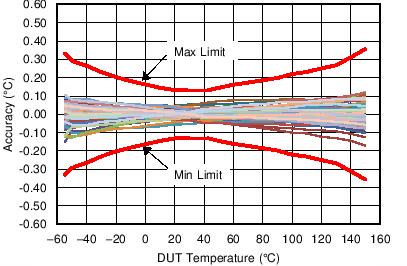
LMT70 LMT70A C001_SNIS187.png
VDD=2.7V
using LUT (Look-Up Table) and linear interporlation for conversion of voltage to temperature
Figure 3. Temperature Accuracy
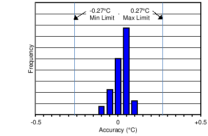
LMT70 LMT70A C003_SNIS187.png
VDD=2.7V
using LUT table for conversion of voltage to temperature
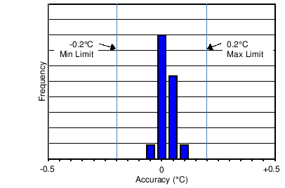
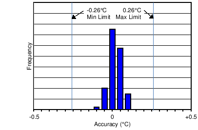
Figure 5. Accuracy Histogram at -40°C
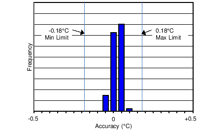
LMT70 LMT70A C002_SNIS187.png
VDD=2.7V
using LUT table for conversion of voltage to temperature
Figure 7. Accuracy Histogram at -10°C
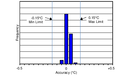
LMT70 LMT70A C006_SNIS187.png
A.
VDD=2.7V
using LUT table for conversion of voltage to temperature
Figure 9. Accuracy Histogram at 50°C
LMT70 LMT70A C008_SNIS187.png
VDD=2.7V
using LUT table for conversion of voltage to temperature
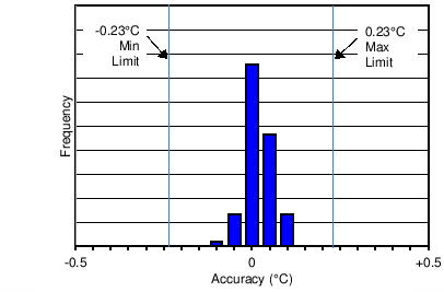
Figure 11. Accuracy Histogram at 110°C
LMT70 LMT70A C010_SNIS187.png
VDD=2.7V
using LUT table for conversion of voltage to temperature
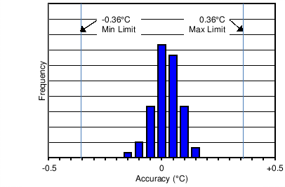
Figure 13. Accuracy Histogram at 150°C
LMT70 LMT70A C011_SNIS187.png
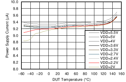
Figure 15. IDD vs Temperature at Various VDD
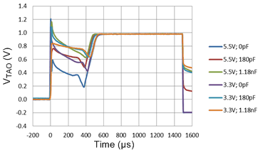
LMT70 LMT70A VDD_ON_Waveform_SNIS187.gif
Conditions: Various VDD and CLOAD
Figure 17. Start-up Response
LMT70 LMT70A C020_SNIS187.png
VDD=2.7V
using LUT table for conversion of voltage to temperature
Figure 19. LMT70A Matching of Adjacent Units on Tape and Reel
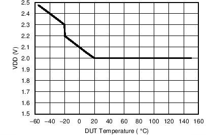
LMT70 LMT70A C018_SNIS187.png
Figure 21. Minimum Recommended Supply Voltage Temperature Sensitivity
LMT70 LMT70A C005_SNIS187.png
VDD=2.7V
using LUT table for conversion of voltage to temperature
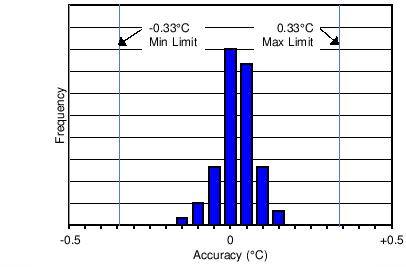
Figure 4. Accuracy Histogram at -55°C
LMT70 LMT70A C0024_SNIS187.png
VDD=2.7V
using LUT table for conversion of voltage to temperature
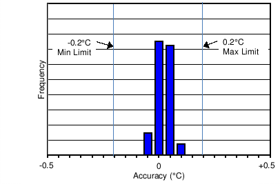
Figure 6. Accuracy Histogram at –20°C
LMT70 LMT70A C004_SNIS187.png
VDD=2.7V
using LUT table for conversion of voltage to temperature
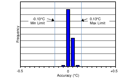
Figure 8. Accuracy Histogram at 30°C
LMT70 LMT70A C007_SNIS187.png
VDD=2.7V
using LUT table for conversion of voltage to temperature
Figure 10. Accuracy Histogram at 90°C
LMT70 LMT70A C009_SNIS187.png
VDD=2.7V
using LUT table for conversion of voltage to temperature
Figure 12. Accuracy Histogram at 120°C
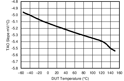
LMT70 LMT70A C013_SNIS187.png
VDD=2.7V
Figure 14. TAO first order transfer function slope vs temperature
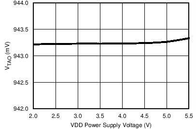
LMT70 LMT70A C012_SNIS187.png
A.
At 30°C
Figure 16. TAO Line Regulation
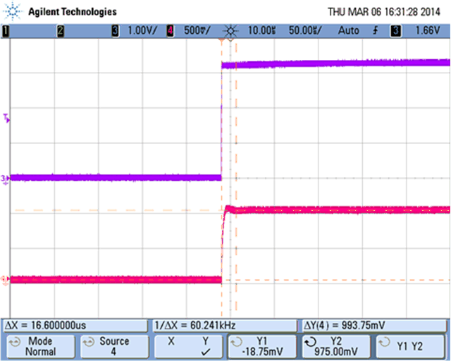
LMT70 LMT70A TON_Waveform_3V_SNIS187.gif
VDD=3.3V
Top trace is T_ON
Bottom trace is TAO
Figure 18. TAO Response to T_ON
LMT70 LMT70A C019_SNIS187.png
at various temperatures
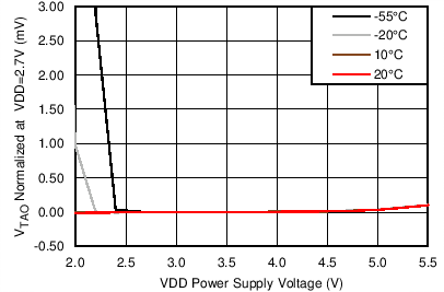
Figure 20. Line Regulation Temperature Variation: VTAO vs Supply Voltage
LMT70 LMT70A C027_SNIS187.png
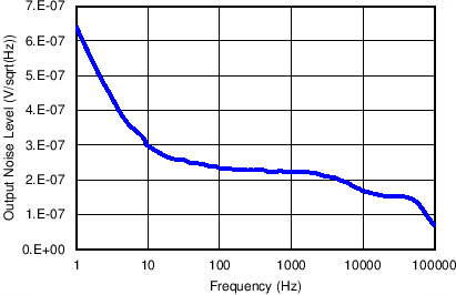
A.
Figure 22. Output Noise vs Frequency