SNOSB45F February 2010 – January 2016 LMV7231
PRODUCTION DATA.
- 1 Features
- 2 Applications
- 3 Description
- 4 Revision History
- 5 Pin Configuration and Functions
- 6 Specifications
- 7 Detailed Description
- 8 Application and Implementation
- 9 Power Supply Recommendations
- 10Layout
- 11Device and Documentation Support
- 12Mechanical, Packaging, and Orderable Information
パッケージ・オプション
メカニカル・データ(パッケージ|ピン)
- RTW|24
サーマルパッド・メカニカル・データ
- RTW|24
発注情報
9 Power Supply Recommendations
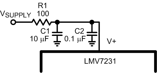
Bypass the supply pin, V+, with a 0.1-μF ceramic capacitor placed close to the V+ pin. If transients with rise or fall times of hundreds of μs and magnitudes of hundreds of mV are expected on the power supply line, an RC lowpass filter network as shown in Figure 40 is recommended for additional bypassing. If no such bypass network is used power supply transients can cause the internal voltage reference of the comparator to temporarily shift potentially resulting in a brief incorrect comparator output. For example, if an RC network with 100-Ω resistance and 10-μF capacitance (1.1-ms rise time) is used the voltage reference temporarily shifts the amount, VTH power supply sensitivity (VTHPSS), specified in the 3.3-V Electrical Characteristics table.
 Figure 40. Power Supply Bypassing