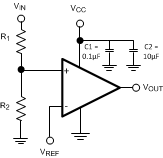
The LMV727x devices are rail-to-rail input low power comparators, characterized at supply voltages 1.8 V, 2.7 V, and 5 V. They consume as little as 9-uA supply current per channel while achieving a 800-ns propagation delay.
The LMV7271 and LMV7275 (single) are available in SC70 and SOT-23 packages. The LMV7272 (dual) is available in the DSBGA package. With these tiny packages, the PCB area can be significantly reduced. They are ideal for low voltage, low power, and space-critical designs.
The LMV7271 and LMV7272 both feature a push-pull output stage which allows operation with minimum power consumption when driving a load.
The LMV7275 features an open-drain output stage that allows for wired-OR configurations. The open-drain output also offers the advantage of allowing the output to be pulled to any voltage up to 5.5 V, regardless of the supply voltage of the LMV7275, which is useful for level-shifting applications.
The LMV727x devices are built with Texas Instruments' advance submicron silicon-gate BiCMOS process. They all have bipolar inputs for improved noise performance, and CMOS outputs for rail-to-rail output swing.
PART NUMBER | PACKAGE | BODY SIZE (NOM) |
---|---|---|
LMV7271, LMV7275 |
SC70 (5) | 1.25 mm × 2.00 mm |
SOT-23 (5) | 1.60 mm × 2.90 mm | |
LMV7272 | DSBGA (8) | 1.50 mm x 1.50 mm |
Changes from H Revision (February 2013) to I Revision
Changes from G Revision (February 2013) to H Revision
PIN | I/O | DESCRIPTION | ||
---|---|---|---|---|
NAME | SOT-23, SC70 | DSBGA | ||
+IN | 1 | — | I | Noninverting Input |
GND | 2 | — | P | Negative Supply Voltage |
-IN | 3 | — | I | Invering Input |
VOUT | 4 | — | O | Output |
V+ | 5 | A2 | P | Positive Supply Voltage |
OUT A | — | A1 | O | Output, Channel A |
-IN A | — | B1 | I | Inverting Input, Channel A |
+IN A | — | C1 | I | Noninverting Input, Channel A |
V- | — | C2 | P | Negative Supply Voltage |
+IN B | — | C3 | I | Noninverting Input, Channel B |
-IN B | — | B3 | I | Inverting Input, Channel B |
OUT B | — | A3 | O | Output, Channel B |
MIN | MAX | UNIT | ||
---|---|---|---|---|
VIN Differential | ±Supply Voltage | V | ||
Supply Voltage (V+ - V−) | 6 | V | ||
Voltage at Input/Output pins | (V+) + 0.1 | (V−) − 0.1 | V | |
Junction Temperature(3) | 150 | °C | ||
Storage Temperature, Tstg | –65 | 150 | °C |
VALUE | UNIT | |||
---|---|---|---|---|
SOT-23, SC70 PACKAGE | ||||
V(ESD) | Electrostatic discharge | Human body model (HBM), per ANSI/ESDA/JEDEC JS-001(1)(2) | ±2000 | V |
Machine Model (MM)(3) | ±200 | |||
DSBGA PACKAGE | ||||
V(ESD) | Electrostatic discharge | Human body model (HBM), per ANSI/ESDA/JEDEC JS-001(1)(2) | ±2000 | V |
Machine Model (MM)(3) | ±200 |
MIN | MAX | UNIT | |
---|---|---|---|
Supply Voltage | 1.8 | 5.5 | V |
Temperature(1) | –40 | 85 | °C |
THERMAL METRIC(1) | LMV7271, LMV7275 | LMV7272 | UNIT | ||
---|---|---|---|---|---|
DBV (SOT-23) | DGK (SC70) | YZR (DSBGA) | |||
5 PINS | 5 PINS | 8 PINS | |||
RθJA | Junction-to-ambient thermal resistance(2) | 325 | 265 | 220 | °C/W |
PARAMETER | CONDITION | MIN(2) | TYP(1) | MAX(2) | UNIT | ||
---|---|---|---|---|---|---|---|
VOS | Input Offset Voltage | 0.3 | 4 | mV | |||
At the temperature extremes | 6 | ||||||
TC VOS | Input Offset Temperature Drift | VCM = 0.9 V (3) | 20 | uV/°C | |||
IB | Input Bias Current | 10 | nA | ||||
IOS | Input Offset Current | 200 | pA | ||||
IS | Supply Current | LMV7271/LMV7275 | 9 | 12 | µA | ||
At the temperature extremes | 14 | ||||||
LMV7272 | 18 | 25 | µA | ||||
At the temperature extremes | 28 | ||||||
ISC | Output Short Circuit Current | Sourcing, VO = 0.9 V (LMV7271/LMV7272 only) |
3.5 | 6 | mA | ||
Sinking, VO = 0.9 V | 4 | 6 | |||||
VOH | Output Voltage High (LMV7271/LMV7272 only) |
IO = 0.5 mA | 1.7 | 1.74 | V | ||
IO = 1.5 mA | 1.47 | 1.63 | |||||
VOL | Output Voltage Low | IO = −0.5 mA | 52 | 100 | mV | ||
IO = −1.5 mA | 166 | 220 | |||||
VCM | Input Common-Mode Voltage Range | CMRR > 45 dB | 1.9 | V | |||
−0.1 | V | ||||||
CMRR | Common-Mode Rejection Ratio | 0 < VCM < 1.8 V | 46 | 78 | dB | ||
PSRR | Power Supply Rejection Ratio | V+ = 1.8 V to 5 V | 55 | 80 | dB | ||
ILEAKAGE | Output Leakage Current | VO = 1.8 V (LMV7275 only) | 2 | pA |
PARAMETER | CONDITION | MIN(2) | TYP(1) | MAX(2) | UNIT | |
---|---|---|---|---|---|---|
tPHL | Propagation Delay (High to Low) |
Input Overdrive = 20 mV Load = 50 pF//5 kΩ |
880 | ns | ||
Input Overdrive = 50 mV Load = 50 pF//5 kΩ |
570 | ns | ||||
tPLH | Propagation Delay (Low to High) |
Input Overdrive = 20 mV Load = 50 pF//5 kΩ |
1100 | ns | ||
Input Overdrive = 50 mV Load = 50 pF//5 kΩ |
800 | ns |
PARAMETER | CONDITIONS | MIN(2) | TYP(1) | MAX(2) | UNIT | ||
---|---|---|---|---|---|---|---|
VOS | Input Offset Voltage | 0.3 | 4 | mV | |||
At the temperature extremes | 6 | ||||||
TC VOS | Input Offset Temperature Drift | VCM = 1.35 V(3) | 20 | µV/°C | |||
IB | Input Bias Current | 10 | nA | ||||
IOS | Input offset Current | 200 | pA | ||||
IS | Supply Current | LMV7271/LMV7275 | 9 | 13 | µA | ||
At the temperature extremes | 15 | ||||||
LMV7272 | 18 | 25 | µA | ||||
At the temperature extremes | 28 | ||||||
ISC | Output Short Circuit Current | Sourcing, VO = 1.35 V (LMV7271/LMV7272 only) |
10 | 15 | mA | ||
Sinking, VO = 1.35 V | 10 | 15 | |||||
VOH | Output Voltage High (LMV7271/LMV7272 only) |
IO = 0.5 mA | 2.63 | 2.66 | V | ||
IO = 2.0 mA | 2.48 | 2.55 | |||||
VOL | Output Voltage Low | IO = −0.5 mA | 50 | 70 | mV | ||
IO = −2 mA | 155 | 220 | |||||
VCM | Input Common Voltage Range | CMRR > 45 dB | 2.8 | V | |||
−0.1 | V | ||||||
CMRR | Common-Mode Rejection Ratio | 0 < VCM < 2.7 V | 46 | 78 | dB | ||
PSRR | Power Supply Rejection Ratio | V+ = 1.8 V to 5 V | 55 | 80 | dB | ||
ILEAKAGE | Output Leakage Current | VO = 2.7 V (LMV7275 only) | 2 | pA |
PARAMETER | CONDITION | MIN(2) | TYP(1) | MAX(2) | UNIT | |
---|---|---|---|---|---|---|
tPHL | Propagation Delay (High to Low) |
Input Overdrive = 20 mV Load = 50 pF//5 kΩ |
1200 | ns | ||
Input Overdrive = 50 mV Load = 50 pF//5 kΩ |
810 | ns | ||||
tPLH | Propagation Delay (Low to High) |
Input Overdrive = 20 mV Load = 50 pF//5 kΩ |
1300 | ns | ||
Input Overdrive = 50 mV Load = 50 pF//5 kΩ |
860 | ns |
PARAMETER | CONDITIONS | MIN(2) | TYP(1) | MAX(2) | UNIT | ||
---|---|---|---|---|---|---|---|
VOS | Input Offset Voltage | 0.3 | 4 | mV | |||
At the temperature extremes | 6 | ||||||
TC VOS | Input Offset Temperature Drift | VCM = 2.5 V(3) | 20 | µV/°C | |||
IB | Input Bias Current | 10 | nA | ||||
IOS | Input Offset Current | 200 | pA | ||||
IS | Supply Current | LMV7271/LMV7275 | 10 | 14 | µA | ||
At the temperature extremes | 16 | ||||||
LMV7272 | 20 | 27 | µA | ||||
At the temperature extremes | 30 | ||||||
ISC | Output Short Circuit Current | Sourcing, VO = 2.5 V (LMV7271/LMV7272 only) |
18 | 34 | mA | ||
Sinking, VO = 2.5 V | 18 | 34 | |||||
VOH | Output Voltage High (LMV7271/LMV7272 only) |
IO = 0.5 mA | 4.93 | 4.96 | V | ||
IO = 4.0 mA | 4.675 | 4.77 | |||||
VOL | Output Voltage Low | IO = −0.5 mA | 27 | 70 | mV | ||
IO = −4.0 mA | 225 | 315 | |||||
VCM | Input Common Voltage Range | CMRR > 45 dB | 5.1 | V | |||
−0.1 | |||||||
CMRR | Common-Mode Rejection Ratio | 0 < VCM < 5.0 V | 46 | 78 | dB | ||
PRSS | Power Supply Rejection Ratio | V+ = 1.8 V to 5 V | 55 | 80 | dB | ||
ILEAKAGE | Output Leakage Current | VO = 5 V (LMV7275 only) | 2 | pA |
PARAMETER | CONDITION | MIN(2) | TYP(1) | MAX(2) | UNIT | |
---|---|---|---|---|---|---|
tPHL | Propagation Delay (High to Low) |
Input Overdrive = 20 mV Load = 50 pF//5 kΩ |
2100 | ns | ||
Input Overdrive = 50 mV Load = 50 pF//5 kΩ |
1380 | ns | ||||
tPLH | Propagation Delay (Low to High) |
Input Overdrive = 20 mV Load = 50 pF//5 kΩ |
1800 | ns | ||
Input Overdrive = 50 mV Load = 50 pF//5 kΩ |
1100 | ns |