SNOSAG6G September 2005 – October 2015 LMV791 , LMV792
PRODUCTION DATA.
- 1 Features
- 2 Applications
- 3 Description
- 4 Revision History
- 5 Pin Configuration and Functions
- 6 Specifications
- 7 Detailed Description
- 8 Application and Implementation
- 9 Power Supply Recommendations
- 10Layout
- 11Device and Documentation Support
- 12Mechanical, Packaging, and Orderable Information
1 Features
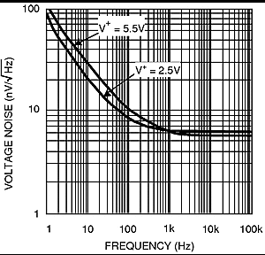
- Input Referred Voltage Noise 5.8 nV/√Hz
- Input Bias Current 100 fA
- Unity Gain Bandwidth 17 MHz
- Supply Current per Channel Enable Mode
- LMV791 1.15 mA
- LMV792 1.30 mA
- Supply Current per Channel in Shutdown Mode 0.02 µA
- Rail-to-Rail Output Swing
- At 10-kΩ Load, 25 mV from Rail
- At 2-kΩ Load, 45 mV from Rail
- Ensured 2.5-V and 5-V Performance
- Total Harmonic Distortion 0.01% at1 kHz, 600 Ω
- Temperature Range −40°C to 125°C
Typical 5-V Supply, Unless Otherwise Noted
2 Applications
- Photodiode Amplifiers
- Active Filters and Buffers
- Low-Noise Signal Processing
- Medical Instrumentation
- Sensor Interface Applications
3 Description
The LMV791 (single) and the LMV792 (dual) low-noise, CMOS input operational amplifiers offer a low input voltage noise density of 5.8 nV/√Hz while consuming only 1.15 mA (LMV791) of quiescent current. The LMV791 and LMV792 are unity gain stable operational amplifiers and have gain bandwidth of 17 MHz. The LMV79x have a supply voltage range of 1.8 V to 5.5 V and can operate from a single supply. The LMV79x each feature a rail-to-rail output stage capable of driving a 600-Ω load and sourcing as much as 60 mA of current.
The LMV79x family provides optimal performance in low-voltage and low-noise systems. A CMOS input stage, with typical input bias currents in the range of a few femtoamperes, and an input common-mode voltage range which includes ground, make the LMV791 and the LMV792 ideal for low-power sensor applications. The LMV79x family has a built-in enable feature which can be used to optimize power dissipation in low power applications.
The LMV791x are manufactured using TI’s advanced VIP50 process and are offered in a 6-pin SOT and a 10-pin VSSOP package respectively.
Device Information(1)
| PART NUMBER | PACKAGE | BODY SIZE (NOM) |
|---|---|---|
| LMV791 | SOT (6) | 2.90 mm × 1.60 mm |
| LMV792 | VSSOP (10) | 3.00 mm × 3.00 mm |
- For all available packages, see the orderable addendum at the end of the data sheet.
Photodiode Transimpedance Amplifier

Low-Noise CMOS Input
