JAJSB28H May 2011 – October 2023 LMZ10501
PRODUCTION DATA
- 1
- 1 特長
- 2 アプリケーション
- 3 概要
- 4 Revision History
- 5 Pin Configuration and Functions
- 6 Specifications
- 7 Detailed Description
- 8 Application and Implementation
- 9 Device and Documentation Support
- 10Mechanical, Packaging, and Orderable Information
パッケージ・オプション
デバイスごとのパッケージ図は、PDF版データシートをご参照ください。
メカニカル・データ(パッケージ|ピン)
- SIL|8
サーマルパッド・メカニカル・データ
発注情報
7.3.3 Output Short Circuit Protection
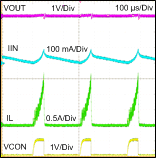
In addition to cycle by cycle current limit, the LMZ10501 features a second level of short circuit protection. If the load pulls the output voltage down and the feedback voltage falls to 0.375 V, the output short circuit protection will engage. In this mode the internal PFET switch is turned OFF after the current limit comparator trips and the beginning of the next cycle is inhibited for approximately 230µs. This forces the inductor current to ramp down and limits excessive current draw from the input supply when the output of the regulator is shorted. The synchronous rectifier is always OFF in this mode. After 230 µs of non-switching a new startup sequence is initiated. During this new startup sequence the current limit is gradually stepped up to the nominal value as illustrated in the Section 7.3.2 section. After the startup sequence is completed again, the feedback voltage is monitored for output short circuit. If the short circuit is still persistent after the new startup sequence, switching will be stopped again and there will be another 230-µs off period. A persistent output short condition results in a hiccup behavior where the LMZ10501 goes through the normal startup sequence, then detects the output short at the end of startup, terminates switching for 230µs, and repeats this cycle until the output short is released. This behavior is illustrated in Figure 7-2.
 Figure 7-2 Hiccup Behavior with Persistent Output Short Circuit.
Because the output current is limited during normal startup by the softstart function, the current charging the output capacitor is also limited. This results in a smooth VOUT ramp up to nominal voltage. However, using excessively large output capacitance or VCON capacitance under normal conditions can prevent the output voltage from reaching 0.375 V at the end of the startup sequence. In such cases the module will maintain the described above hiccup mode and the output voltage will not ramp up to final value. To cause this condition, one can have to use unnecessarily large output capacitance for 1A load applications. See the Section 8.2.2.5 section for guidance on maximum capacitances for different output voltage settings.