JAJSB28H May   2011  – October 2023 LMZ10501

PRODUCTION DATA  

  1.   1
  2. 特長
  3. アプリケーション
  4. 概要
  5. Revision History
  6. Pin Configuration and Functions
  7. Specifications
    1. 6.1 Absolute Maximum Ratings
    2. 6.2 ESD Ratings
    3. 6.3 Recommended Operating Conditions
    4. 6.4 Thermal Information
    5. 6.5 Electrical Characteristics
    6. 6.6 System Characteristics
    7. 6.7 Typical Characteristics
  8. Detailed Description
    1. 7.1 Overview
    2. 7.2 Functional Block Diagram
    3. 7.3 Feature Description
      1. 7.3.1 Current Limit
      2. 7.3.2 Startup Behavior and Soft Start
      3. 7.3.3 Output Short Circuit Protection
      4. 7.3.4 Thermal Overload Protection
    4. 7.4 Device Functional Modes
      1. 7.4.1 Circuit Operation
      2. 7.4.2 Input Under Voltage Detection
      3. 7.4.3 Shutdown Mode
      4. 7.4.4 EN Pin Operation
      5. 7.4.5 Internal Synchronous Rectification
      6. 7.4.6 High Duty Cycle Operation
  9. Application and Implementation
    1. 8.1 Application Information
    2. 8.2 Typical Application
      1. 8.2.1 Design Requirements
      2. 8.2.2 Detailed Design Procedure
        1. 8.2.2.1 Custom Design With WEBENCH® Tools
        2. 8.2.2.2 Setting The Output Voltage
          1. 8.2.2.2.1 RT And RB Selection For Fixed VOUT
          2. 8.2.2.2.2 Output Voltage Accuracy Optimization
        3. 8.2.2.3 Dynamic Output Voltage Scaling
        4. 8.2.2.4 Integrated Inductor
        5. 8.2.2.5 Input And Output Capacitor Selection
      3. 8.2.3 Application Curves
        1. 8.2.3.1 VOUT = 1.2 V
        2. 8.2.3.2 VOUT = 1.8 V
        3. 8.2.3.3 VOUT = 2.5 V
        4. 8.2.3.4 VOUT = 3.3 V
    3. 8.3 Power Supply Recommendations
      1. 8.3.1 Voltage Range
      2. 8.3.2 Current Capability
      3. 8.3.3 Input Connection
        1. 8.3.3.1 Voltage Drops
        2. 8.3.3.2 Stability
    4. 8.4 Layout
      1. 8.4.1 Layout Guidelines
      2. 8.4.2 Layout Example
      3. 8.4.3 Package Considerations
  10. Device and Documentation Support
    1. 9.1 Device Support
      1. 9.1.1 Custom Design With WEBENCH® Tools
    2. 9.2 Documentation Support
      1. 9.2.1 Related Documentation
    3. 9.3 ドキュメントの更新通知を受け取る方法
    4. 9.4 サポート・リソース
    5. 9.5 Trademarks
    6. 9.6 静電気放電に関する注意事項
    7. 9.7 用語集
  11. 10Mechanical, Packaging, and Orderable Information

パッケージ・オプション

デバイスごとのパッケージ図は、PDF版データシートをご参照ください。

メカニカル・データ(パッケージ|ピン)
  • SIL|8
サーマルパッド・メカニカル・データ
発注情報

Startup Behavior and Soft Start

The LMZ10501 features a current limit based soft start circuit in order to prevent large in-rush current and output overshoot as VOUT is ramping up. This is achieved by gradually increasing the PFET current limit threshold to the final operating value as the output voltage ramps during startup. The maximum allowed current in the inductor is stepped up in a staircase profile for a fixed number of switching periods in each step. Additionally, the switching frequency in the first step is set at 450kHz and is then increased for each of the following steps until it reaches 2MHz at the final step of current limiting. This current limiting behavior is illustrated in Figure 7-1 and allows for a smooth VOUT ramp up.
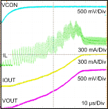
GUID-9F2E431F-4BBB-4196-A1F1-E56DCDFE0556-low.gifFigure 7-1 Startup Behavior of Current Limit Based Softstart.

The soft start rate is also limited by the VCON ramp up rate. The VCON pin is discharged internally through a pull down device before startup occurs. This is done to deplete any residual charge on the VCON filter capacitor and allow the VCON voltage to ramp up from 0V when the part is started. The events that cause VCON discharge are thermal shutdown, UVLO, EN low, or output short circuit detection. The minimum recommended capacitance on VCON is 220pF and the maximum is 1nF. The duration of startup current limiting sequence takes approximately 75µs. After the sequence is completed, the feedback voltage is monitored for output short circuit events.