JAJSH78J June   2010  – April 2019 LMZ10503EXT

PRODUCTION DATA.  

  1. 特長
  2. アプリケーション
  3. 概要
    1.     Device Images
      1.      代表的なアプリケーション回路
      2.      VOUT = 3.3Vでの効率
  4. 改訂履歴
  5. 概要(続き)
  6. Pin Configuration and Functions
    1.     Pin Functions
  7. Specifications
    1. 7.1 Absolute Maximum Ratings
    2. 7.2 ESD Ratings
    3. 7.3 Recommended Operating Conditions
    4. 7.4 Thermal Information
    5. 7.5 Electrical Characteristics
    6. 7.6 Typical Characteristics
  8. Detailed Description
    1. 8.1 Overview
    2. 8.2 Functional Block Diagram
    3. 8.3 Feature Description
      1. 8.3.1 Enable
      2. 8.3.2 Enable and UVLO
      3. 8.3.3 Soft-Start
      4. 8.3.4 Soft-Start Capacitor
      5. 8.3.5 Tracking
      6. 8.3.6 Tracking - Equal Soft-Start Time
      7. 8.3.7 Tracking - Equal Slew Rates
      8. 8.3.8 Current Limit
      9. 8.3.9 Overtemperature Protection
    4. 8.4 Device Functional Modes
      1. 8.4.1 Prebias Start-Up Capability
  9. Application and Implementation
    1. 9.1 Application Information
    2. 9.2 Typical Application
      1. 9.2.1 Design Requirements
      2. 9.2.2 Detailed Design Procedure
        1. 9.2.2.1 Custom Design With WEBENCH® Tools
        2. 9.2.2.2 Input Capacitor Selection
        3. 9.2.2.3 Output Capacitor Selection
          1. 9.2.2.3.1 Output Voltage Setting
        4. 9.2.2.4 Loop Compensation
      3. 9.2.3 Application Curves
    3. 9.3 System Examples
      1. 9.3.1 Application Schematic for 3.3-V to 5-V Input and 2.5-V Output With Optimized Ripple and Transient Response
      2. 9.3.2 Application Schematic for 3.3-V to 5-V Input and 2.5-V Output
      3. 9.3.3 EMI Tested Schematic for 2.5-V Output Based on 3.3-V to 5-V Input
  10. 10Power Supply Recommendations
  11. 11Layout
    1. 11.1 Layout Guidelines
    2. 11.2 Layout Examples
    3. 11.3 Estimate Power Dissipation and Thermal Considerations
    4. 11.4 Power Module SMT Guidelines
  12. 12デバイスおよびドキュメントのサポート
    1. 12.1 デバイス・サポート
      1. 12.1.1 デベロッパー・ネットワークの製品に関する免責事項
      2. 12.1.2 開発サポート
        1. 12.1.2.1 WEBENCH®ツールによるカスタム設計
    2. 12.2 ドキュメントのサポート
      1. 12.2.1 関連資料
    3. 12.3 コミュニティ・リソース
    4. 12.4 商標
    5. 12.5 静電気放電に関する注意事項
    6. 12.6 Glossary
  13. 13メカニカル、パッケージ、および注文情報

パッケージ・オプション

メカニカル・データ(パッケージ|ピン)
サーマルパッド・メカニカル・データ
発注情報

Enable and UVLO

Using a resistor divider from VIN to EN as shown in the schematic diagram below, the input voltage at which the part begins switching can be increased above the normal input UVLO level according to:

Equation 1. LMZ10503EXT eq_3_SNVS610.gif

For example, suppose that the required input UVLO level is 3.69 V. Choosing Renb = 10 kΩ, then we calculate Rent = 20 kΩ.
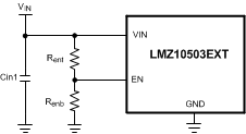
LMZ10503EXT 30118244.gifFigure 16. Setting Enable and UVLO

Alternatively, the EN pin can be driven from another voltage source to cater to system sequencing requirements commonly found in FPGA and other multi-rail applications. Figure 17 shows an LMZ10503EXT that is sequenced to start based on the voltage level of a master system rail (VOUT1).
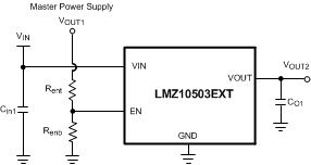
LMZ10503EXT 30118245.gifFigure 17. Setting Enable and UVLO Using External Power Supply