JAJSH78J June 2010 – April 2019 LMZ10503EXT
PRODUCTION DATA.
- 1 特長
- 2 アプリケーション
- 3 概要
- 4 改訂履歴
- 5 概要(続き)
- 6 Pin Configuration and Functions
- 7 Specifications
- 8 Detailed Description
- 9 Application and Implementation
- 10Power Supply Recommendations
- 11Layout
- 12デバイスおよびドキュメントのサポート
- 13メカニカル、パッケージ、および注文情報
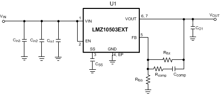
9.3.3 EMI Tested Schematic for 2.5-V Output Based on 3.3-V to 5-V Input
The compensation for each solution was optimized to work over the full input range. Many applications have a fixed input voltage rail. It is possible to modify the compensation to obtain a faster transient response for a given input voltage operating point.
 Figure 28. EMI Tested Schematic for 2.5-V Output Based on 3.3-V to 5-V Input
 Table 9. Bill of Materials, VIN = 5 V, VOUT = 2.5 V, IOUT (MAX) = 3 A,
Tested With EN55022 Class B Radiated Emissions
| DESIGNATOR | DESCRIPTION | CASE SIZE | MANUFACTURER | MANUFACTURER P/N | QUANTITY |
|---|---|---|---|---|---|
| U1 | Power module | PFM-7 | Texas Instruments | LMZ10503EXTTZ | 1 |
| Cin1 | 1 µF, X7R, 16 V | 0805 | TDK | C2012X7R1C105K | 1 |
| Cin2 | 4.7 µF, X5R, 6.3 V | 0805 | TDK | C2012X5R0J475K | 1 |
| Cin3 | 47 µF, X5R, 6.3 V | 1210 | TDK | C3225X5R0J476M | 1 |
| CO1 | 100 µF, X5R, 6.3 V | 1812 | TDK | C4532X5R0J107M | 1 |
| Rfbt | 75 kΩ | 0805 | Vishay Dale | CRCW080575K0FKEA | 1 |
| Rfbb | 34.8 kΩ | 0805 | Vishay Dale | CRCW080534K8FKEA | 1 |
| Rcomp | 1.1 kΩ | 0805 | Vishay Dale | CRCW08051K10FKEA | 1 |
| Ccomp | 180 pF, ±5%, C0G, 50 V | 0603 | TDK | C1608C0G1H181J | 1 |
| CSS | 10 nF, ±5%, C0G, 50 V | 0805 | TDK | C2012C0G1H103J | 1 |
Table 10. Output Voltage Setting (Rfbt = 75 kΩ)
| VOUT | Rfbb |
|---|---|
| 3.3 V | 23.7 kΩ |
| 2.5 V | 34.8 kΩ |
| 1.8 V | 59 kΩ |
| 1.5 V | 84.5 kΩ |
| 1.2 V | 150 kΩ |
| 0.9 V | 590 kΩ |