JAJSH78J June   2010  – April 2019 LMZ10503EXT

PRODUCTION DATA.  

  1. 特長
  2. アプリケーション
  3. 概要
    1.     Device Images
      1.      代表的なアプリケーション回路
      2.      VOUT = 3.3Vでの効率
  4. 改訂履歴
  5. 概要(続き)
  6. Pin Configuration and Functions
    1.     Pin Functions
  7. Specifications
    1. 7.1 Absolute Maximum Ratings
    2. 7.2 ESD Ratings
    3. 7.3 Recommended Operating Conditions
    4. 7.4 Thermal Information
    5. 7.5 Electrical Characteristics
    6. 7.6 Typical Characteristics
  8. Detailed Description
    1. 8.1 Overview
    2. 8.2 Functional Block Diagram
    3. 8.3 Feature Description
      1. 8.3.1 Enable
      2. 8.3.2 Enable and UVLO
      3. 8.3.3 Soft-Start
      4. 8.3.4 Soft-Start Capacitor
      5. 8.3.5 Tracking
      6. 8.3.6 Tracking - Equal Soft-Start Time
      7. 8.3.7 Tracking - Equal Slew Rates
      8. 8.3.8 Current Limit
      9. 8.3.9 Overtemperature Protection
    4. 8.4 Device Functional Modes
      1. 8.4.1 Prebias Start-Up Capability
  9. Application and Implementation
    1. 9.1 Application Information
    2. 9.2 Typical Application
      1. 9.2.1 Design Requirements
      2. 9.2.2 Detailed Design Procedure
        1. 9.2.2.1 Custom Design With WEBENCH® Tools
        2. 9.2.2.2 Input Capacitor Selection
        3. 9.2.2.3 Output Capacitor Selection
          1. 9.2.2.3.1 Output Voltage Setting
        4. 9.2.2.4 Loop Compensation
      3. 9.2.3 Application Curves
    3. 9.3 System Examples
      1. 9.3.1 Application Schematic for 3.3-V to 5-V Input and 2.5-V Output With Optimized Ripple and Transient Response
      2. 9.3.2 Application Schematic for 3.3-V to 5-V Input and 2.5-V Output
      3. 9.3.3 EMI Tested Schematic for 2.5-V Output Based on 3.3-V to 5-V Input
  10. 10Power Supply Recommendations
  11. 11Layout
    1. 11.1 Layout Guidelines
    2. 11.2 Layout Examples
    3. 11.3 Estimate Power Dissipation and Thermal Considerations
    4. 11.4 Power Module SMT Guidelines
  12. 12デバイスおよびドキュメントのサポート
    1. 12.1 デバイス・サポート
      1. 12.1.1 デベロッパー・ネットワークの製品に関する免責事項
      2. 12.1.2 開発サポート
        1. 12.1.2.1 WEBENCH®ツールによるカスタム設計
    2. 12.2 ドキュメントのサポート
      1. 12.2.1 関連資料
    3. 12.3 コミュニティ・リソース
    4. 12.4 商標
    5. 12.5 静電気放電に関する注意事項
    6. 12.6 Glossary
  13. 13メカニカル、パッケージ、および注文情報

パッケージ・オプション

メカニカル・データ(パッケージ|ピン)
サーマルパッド・メカニカル・データ
発注情報

Power Module SMT Guidelines

The recommendations below are for a standard module surface mount assembly

  • Land Pattern – Follow the PCB land pattern with either soldermask defined or non-soldermask defined pads
  • Stencil Aperture
    • For the exposed die attach pad (DAP), adjust the stencil for approximately 80% coverage of the PCB land pattern
    • For all other I/O pads use a 1:1 ratio between the aperture and the land pattern recommendation
  • Solder Paste – Use a standard SAC Alloy such as SAC 305, type 3 or higher
  • Stencil Thickness – 0.125 to 0.15 mm
  • Reflow - Refer to solder paste supplier recommendation and optimized per board size and density
  • Maximum number of reflows allowed is one
  • Refer to AN Design Summary LMZ1xxx and LMZ2xxx Power Modules Family (SNAA214) for reflow information.
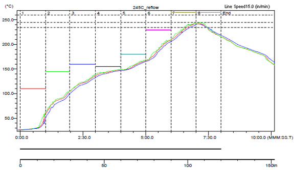
LMZ10503EXT reflow_chart_snvs632.pngFigure 35. Sample Reflow Profile

Table 11. Sample Reflow Profile Table

PROBE MAX TEMP (°C) REACHED MAX TEMP TIME ABOVE 235°C REACHED 235°C TIME ABOVE 245°C REACHED 245°C TIME ABOVE 260°C REACHED 260°C
1 242.5 6.58 0.49 6.39 0.00 0.00
2 242.5 7.10 0.55 6.31 0.00 7.10 0.00
3 241.0 7.09 0.42 6.44 0.00 0.00