JAJSB08P December   2009  – April 2019 LMZ10504

PRODUCTION DATA.  

  1. 特長
  2. アプリケーション
  3. 概要
    1.     Device Images
      1.      代表的なアプリケーション回路
      2.      VOUT = 3.3Vでの効率
  4. 改訂履歴
  5. Pin Configuration and Functions
    1.     Pin Functions
  6. Specifications
    1. 6.1 Absolute Maximum Ratings
    2. 6.2 ESD Ratings
    3. 6.3 Recommended Operating Conditions
    4. 6.4 Thermal Information
    5. 6.5 Electrical Characteristics
    6. 6.6 Typical Characteristics
  7. Detailed Description
    1. 7.1 Overview
    2. 7.2 Functional Block Diagram
    3. 7.3 Feature Description
      1. 7.3.1 Enable
      2. 7.3.2 Enable and UVLO
      3. 7.3.3 Soft-Start
      4. 7.3.4 Soft-Start Capacitor
      5. 7.3.5 Tracking
      6. 7.3.6 Tracking - Equal Soft-Start Time
      7. 7.3.7 Tracking - Equal Slew Rates
      8. 7.3.8 Current Limit
      9. 7.3.9 Overtemperature Protection
    4. 7.4 Device Functional Modes
      1. 7.4.1 Prebias Start-Up Capability
  8. Application and Implementation
    1. 8.1 Application Information
    2. 8.2 Typical Application
      1. 8.2.1 Design Requirements
      2. 8.2.2 Detailed Design Procedure
        1. 8.2.2.1 Custom Design With WEBENCH® Tools
        2. 8.2.2.2 Input Capacitor Selection
        3. 8.2.2.3 Output Capacitor Selection
          1. 8.2.2.3.1 Output Voltage Setting
        4. 8.2.2.4 Loop Compensation
      3. 8.2.3 Application Curves
    3. 8.3 System Examples
      1. 8.3.1 Application Schematic for 3.3-V to 5-V Input and 2.5-V Output With Optimized Ripple and Transient Response
      2. 8.3.2 Application Schematic for 3.3-V to 5-V Input and 2.5-V Output
      3. 8.3.3 EMI Tested Schematic for 2.5-V Output Based on 3.3-V to 5-V Input
  9. Power Supply Recommendations
  10. 10Layout
    1. 10.1 Layout Guidelines
    2. 10.2 Layout Examples
    3. 10.3 Estimate Power Dissipation and Thermal Considerations
    4. 10.4 Power Module SMT Guidelines
  11. 11デバイスおよびドキュメントのサポート
    1. 11.1 デバイス・サポート
      1. 11.1.1 デベロッパー・ネットワークの製品に関する免責事項
      2. 11.1.2 開発サポート
        1. 11.1.2.1 WEBENCH®ツールによるカスタム設計
    2. 11.2 ドキュメントのサポート
      1. 11.2.1 関連資料
    3. 11.3 ドキュメントの更新通知を受け取る方法
    4. 11.4 コミュニティ・リソース
    5. 11.5 商標
    6. 11.6 静電気放電に関する注意事項
    7. 11.7 Glossary
  12. 12メカニカル、パッケージ、および注文情報

パッケージ・オプション

メカニカル・データ(パッケージ|ピン)
サーマルパッド・メカニカル・データ
発注情報

Tracking - Equal Slew Rates

Alternatively, the tracking feature can be used to have similar output voltage ramp rates. This is referred to as simultaneous start-up. In this case, the tracking resistors can be determined based on Equation 5:

Equation 5. LMZ10504 eq_6_SNVS610.gif

and to ensure proper overdrive of the SS pin

Equation 6. LMZ10504 eq_7_SNVS610.gif

For the example case of VOUT1 = 5 V and VOUT2 = 2.5 V, with Rtrkt set to 33 kΩ as before, Rtrkb is calculated from the above equation to be 15.5 kΩ. Figure 20 shows an example of tracking using the equal slew rates.
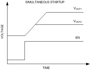
LMZ10504 30088261.gifFigure 20. Timing Diagram for Tracking Using Equal Slew Rates