JAJSBZ7E JULY   2013  – December 2019 LMZ31710

PRODUCTION DATA.  

  1. 特長
  2. アプリケーション
  3. 概要
    1.     Device Images
      1.      アプリケーション概略図
  4. 改訂履歴
  5. Pin Configuration and Functions
    1.     Pin Functions
  6. Specifications
    1. 6.1 Absolute Maximum Ratings
    2. 6.2 ESD Ratings
    3. 6.3 Recommended Operating Conditions
    4. 6.4 Thermal Information
    5. 6.5 Electrical Characteristics
    6. 6.6 Typical Characteristics (PVIN = VIN = 12 V)
    7. 6.7 Typical Characteristics (PVIN = VIN = 5 V)
    8. 6.8 Typical Characteristics (PVIN = 3.3 V, VIN = 5 V)
  7. Detailed Description
    1. 7.1 Overview
    2. 7.2 Functional Block Diagram
    3. 7.3 Feature Description
      1. 7.3.1  VIN and PVIN Input Voltage
      2. 7.3.2  3.3-V PVIN Operation
      3. 7.3.3  Adjusting the Output Voltage (0.6 V to 5.5 V)
      4. 7.3.4  Capacitor Recommendations For the LMZ31710 Power Supply
        1. 7.3.4.1 Capacitor Technologies
          1. 7.3.4.1.1 Electrolytic, Polymer-Electrolytic Capacitors
          2. 7.3.4.1.2 Ceramic Capacitors
          3. 7.3.4.1.3 Tantalum, Polymer-Tantalum Capacitors
        2. 7.3.4.2 Input Capacitor
        3. 7.3.4.3 Output Capacitor
      5. 7.3.5  Transient Response
        1. 7.3.5.1 Transient Response Waveforms
      6. 7.3.6  Power Good (PWRGD)
      7. 7.3.7  Light Load Efficiency (LLE)
      8. 7.3.8  SYNC_OUT
      9. 7.3.9  Parallel Operation
      10. 7.3.10 Power-Up Characteristics
      11. 7.3.11 Pre-Biased Start-Up
      12. 7.3.12 Remote Sense
      13. 7.3.13 Thermal Shutdown
      14. 7.3.14 Output On/Off Inhibit (INH)
      15. 7.3.15 Slow Start (SS/TR)
      16. 7.3.16 Overcurrent Protection
      17. 7.3.17 Synchronization (CLK)
      18. 7.3.18 Sequencing (SS/TR)
    4. 7.4 Device Functional Modes
      1. 7.4.1 Programmable Undervoltage Lockout (UVLO)
  8. Application and Implementation
    1. 8.1 Application Information
    2. 8.2 Typical Application
      1. 8.2.1 Design Requirements
      2. 8.2.2 Detailed Design Procedure
        1. 8.2.2.1 Custom Design With WEBENCH® Tools
        2. 8.2.2.2 Setting The Output Voltage
        3. 8.2.2.3 Setting the Switching Frequency
        4. 8.2.2.4 Input Capacitance
        5. 8.2.2.5 Output Capacitance
    3. 8.3 Additional Application Schematics
  9. Power Supply Recommendations
  10. 10Layout
    1. 10.1 Layout Considerations
    2. 10.2 Layout Examples
      1. 10.2.1 EMI
  11. 11デバイスおよびドキュメントのサポート
    1. 11.1 デバイス・サポート
      1. 11.1.1 開発サポート
        1. 11.1.1.1 WEBENCH®ツールによるカスタム設計
      2. 11.1.2 デベロッパー・ネットワークの製品に関する免責事項
    2. 11.2 ドキュメントのサポート
      1. 11.2.1 関連資料
    3. 11.3 ドキュメントの更新通知を受け取る方法
    4. 11.4 サポート・リソース
    5. 11.5 商標
    6. 11.6 静電気放電に関する注意事項
    7. 11.7 Glossary
  12. 12メカニカル、パッケージ、および注文情報
    1. 12.1 Tape and Reel Information

パッケージ・オプション

メカニカル・データ(パッケージ|ピン)
サーマルパッド・メカニカル・データ
発注情報

Parallel Operation

Up to six LMZ31710 devices can be paralleled for increased output current. Multiple connections must be made between the paralleled devices and the component selection is slightly different than for a stand-alone LMZ31710 device. A typical LMZ31710 parallel schematic is shown in Figure 23. Refer to application note, SNVA695 for information and design help when paralleling multiple LMZ31710 devices. Additionally, an EVM featuring two LMZ31710 devices operating in parallel can be evaluated using the LMZ31710X2EVM.
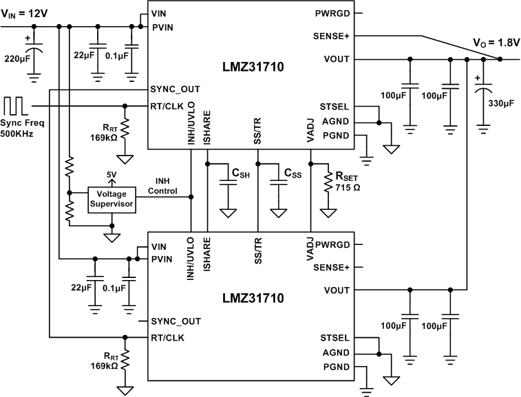
LMZ31710 LMZ31710 Dual Parallel.gifFigure 23. Typical LMZ31710 Parallel Schematic