JAJSBZ7E JULY 2013 – December 2019 LMZ31710
PRODUCTION DATA.
- 1 特長
- 2 アプリケーション
- 3 概要
- 4 改訂履歴
- 5 Pin Configuration and Functions
- 6 Specifications
-
7 Detailed Description
- 7.1 Overview
- 7.2 Functional Block Diagram
- 7.3
Feature Description
- 7.3.1 VIN and PVIN Input Voltage
- 7.3.2 3.3-V PVIN Operation
- 7.3.3 Adjusting the Output Voltage (0.6 V to 5.5 V)
- 7.3.4 Capacitor Recommendations For the LMZ31710 Power Supply
- 7.3.5 Transient Response
- 7.3.6 Power Good (PWRGD)
- 7.3.7 Light Load Efficiency (LLE)
- 7.3.8 SYNC_OUT
- 7.3.9 Parallel Operation
- 7.3.10 Power-Up Characteristics
- 7.3.11 Pre-Biased Start-Up
- 7.3.12 Remote Sense
- 7.3.13 Thermal Shutdown
- 7.3.14 Output On/Off Inhibit (INH)
- 7.3.15 Slow Start (SS/TR)
- 7.3.16 Overcurrent Protection
- 7.3.17 Synchronization (CLK)
- 7.3.18 Sequencing (SS/TR)
- 7.4 Device Functional Modes
- 8 Application and Implementation
- 9 Power Supply Recommendations
- 10Layout
- 11デバイスおよびドキュメントのサポート
- 12メカニカル、パッケージ、および注文情報
7.3.16 Overcurrent Protection
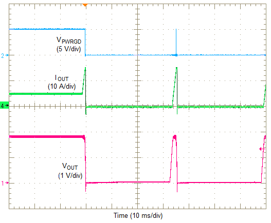
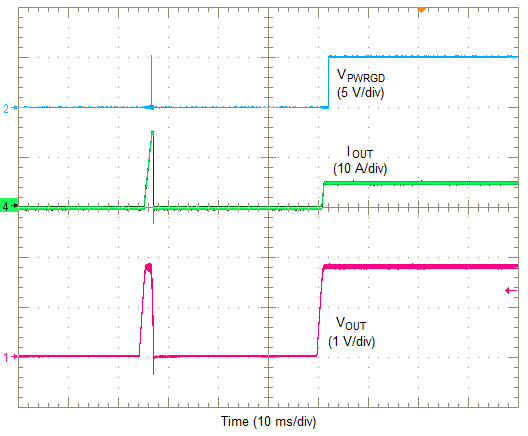
For protection against load faults, the LMZ31710 incorporates output overcurrent protection. The overcurrent protection mode can be selected using the OCP_SEL pin. Leaving the OCP_SEL pin open selects hiccup mode and connecting it to AGND selects cycle-by-cycle mode. In hiccup mode, applying a load that exceeds the overcurrent threshold of the regulator causes the regulated output to shut down. Following shutdown, the module periodically attempts to recover by initiating a soft-start power-up as shown in Figure 30. This is described as a hiccup mode of operation, whereby the module continues in a cycle of successive shutdown and power up until the load fault is removed. During this period, the average current flowing into the fault is significantly reduced which reduces power dissipation. Once the fault is removed, the module automatically recovers and returns to normal operation as shown in Figure 31.
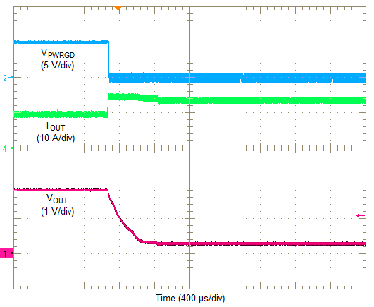
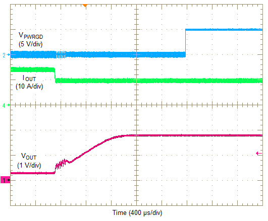
In cycle-by-cycle mode, applying a load that exceeds the regulator's overcurrent threshold limits the output current and reduces the output voltage as shown in Figure 32. During this period, the current flowing into the fault remains high causing the power dissipation to stay high as well. Once the overcurrent condition is removed, the output voltage returns to the set-point voltage as shown in Figure 33.
 Figure 30. Overcurrent Limiting (Hiccup)
  Figure 32. Overcurrent Limiting (Cycle-By-Cycle)
  Figure 31. Removal Of Overcurrent (Hiccup)
  Figure 33. Removal Of Overcurrent (Cycle-By-Cycle)