JAJSF76D September   2015  – June 2018 LMZ36002

PRODUCTION DATA.  

  1. 特長
  2. アプリケーション
  3. 概要
    1.     Device Images
      1.      アプリケーション概略図
      2.      効率と出力電流との関係
  4. 改訂履歴
  5. Pin Configuration and Functions
    1.     Pin Functions
  6. Specifications
    1. 6.1  Absolute Maximum Ratings
    2. 6.2  ESD Ratings
    3. 6.3  Recommended Operating Conditions
    4. 6.4  Thermal Information
    5. 6.5  Electrical Characteristics
    6. 6.6  Switching Characteristics
    7. 6.7  Typical Characteristics
    8. 6.8  Typical Characteristics
    9. 6.9  Typical Characteristics
    10. 6.10 Typical Characteristics (Thermal Derating)
  7. Detailed Description
    1. 7.1 Overview
    2. 7.2 Functional Block Diagram
    3. 7.3 Feature Description
      1. 7.3.1  Adjusting the Output Voltage
      2. 7.3.2  Switching Frequency (RT)
      3. 7.3.3  Recommended Operating Range
      4. 7.3.4  Synchronization (CLK)
      5. 7.3.5  Output Capacitor Selection
      6. 7.3.6  VERSA-COMP Pin Configurations
      7. 7.3.7  Input Capacitor Selection
      8. 7.3.8  Output On/Off Inhibit (INH/UVLO)
      9. 7.3.9  Under Voltage Lockout (UVLO)
      10. 7.3.10 Remote Sense
      11. 7.3.11 VBSEL
      12. 7.3.12 Soft-Start (SS/TR)
      13. 7.3.13 Power Good (PWRGD) and Pull-up (PWRGD_PU)
      14. 7.3.14 Overcurrent Protection
      15. 7.3.15 Thermal Shutdown
    4. 7.4 Device Functional Modes
      1. 7.4.1 Active Mode
      2. 7.4.2 Light Load Operation
      3. 7.4.3 Shutdown Mode
  8. Application and Implementation
    1. 8.1 Application Information
      1. 8.1.1 Minimum External Component Application
        1. 8.1.1.1 Design Requirements
        2. 8.1.1.2 Detailed Design Procedure
          1. 8.1.1.2.1 Custom Design With WEBENCH® Tools
          2. 8.1.1.2.2 Output Voltage Set-Point
          3. 8.1.1.2.3 RT and RTSEL
          4. 8.1.1.2.4 VERSA-COMP
          5. 8.1.1.2.5 VBSEL
          6. 8.1.1.2.6 Input Capacitors
          7. 8.1.1.2.7 Output Capacitors
          8. 8.1.1.2.8 Application Curves
      2. 8.1.2 Typical Application
        1. 8.1.2.1 Design Requirements
      3. 8.1.3 Detailed Design Procedure
        1. 8.1.3.1 Switching Frequency
        2. 8.1.3.2 Power Good
        3. 8.1.3.3 Inhibit Control
        4. 8.1.3.4 VERSA-COMP
        5. 8.1.3.5 VBSEL
        6. 8.1.3.6 Soft-Start Capacitors
        7. 8.1.3.7 Input Capacitors
        8. 8.1.3.8 Output Capacitors
  9. Power Supply Recommendations
  10. 10Layout
    1. 10.1 Layout Guidelines
    2. 10.2 Layout Example
    3. 10.3 EMI
  11. 11デバイスおよびドキュメントのサポート
    1. 11.1 デバイス・サポート
      1. 11.1.1 開発サポート
        1. 11.1.1.1 WEBENCH®ツールによるカスタム設計
      2. 11.1.2 デベロッパー・ネットワークの製品に関する免責事項
    2. 11.2 ドキュメントの更新通知を受け取る方法
    3. 11.3 コミュニティ・リソース
    4. 11.4 商標
    5. 11.5 静電気放電に関する注意事項
    6. 11.6 Glossary
  12. 12メカニカル、パッケージ、および注文情報

パッケージ・オプション

メカニカル・データ(パッケージ|ピン)
サーマルパッド・メカニカル・データ
発注情報

EMI

The LMZ36002 is compliant with EN55022 Class B radiated emissions. Figure 42 through Figure 45 show typical examples of radiated emissions plots for the LMZ36002 operating from 24 V and 48 V. Both graphs include the plots of the antenna in the horizontal and vertical positions.
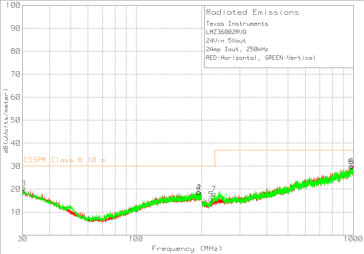
LMZ36002 EMI_24Vin_5Vout_LMZ36002.pngFigure 42. Radiated Emissions (EN55022 Class B)
24-V Input, 5-V Output, 2-A Load, 250 kHz
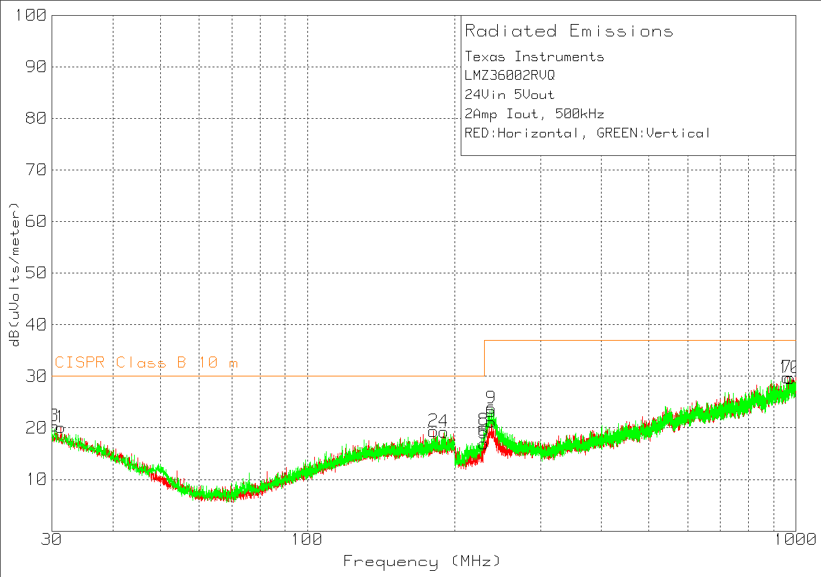
LMZ36002 EMI_24Vin_5Vout_500kHzLMZ36002.pngFigure 44. Radiated Emissions (EN55022 Class B)
24-V Input, 5-V Output, 2-A Load, 500 kHz
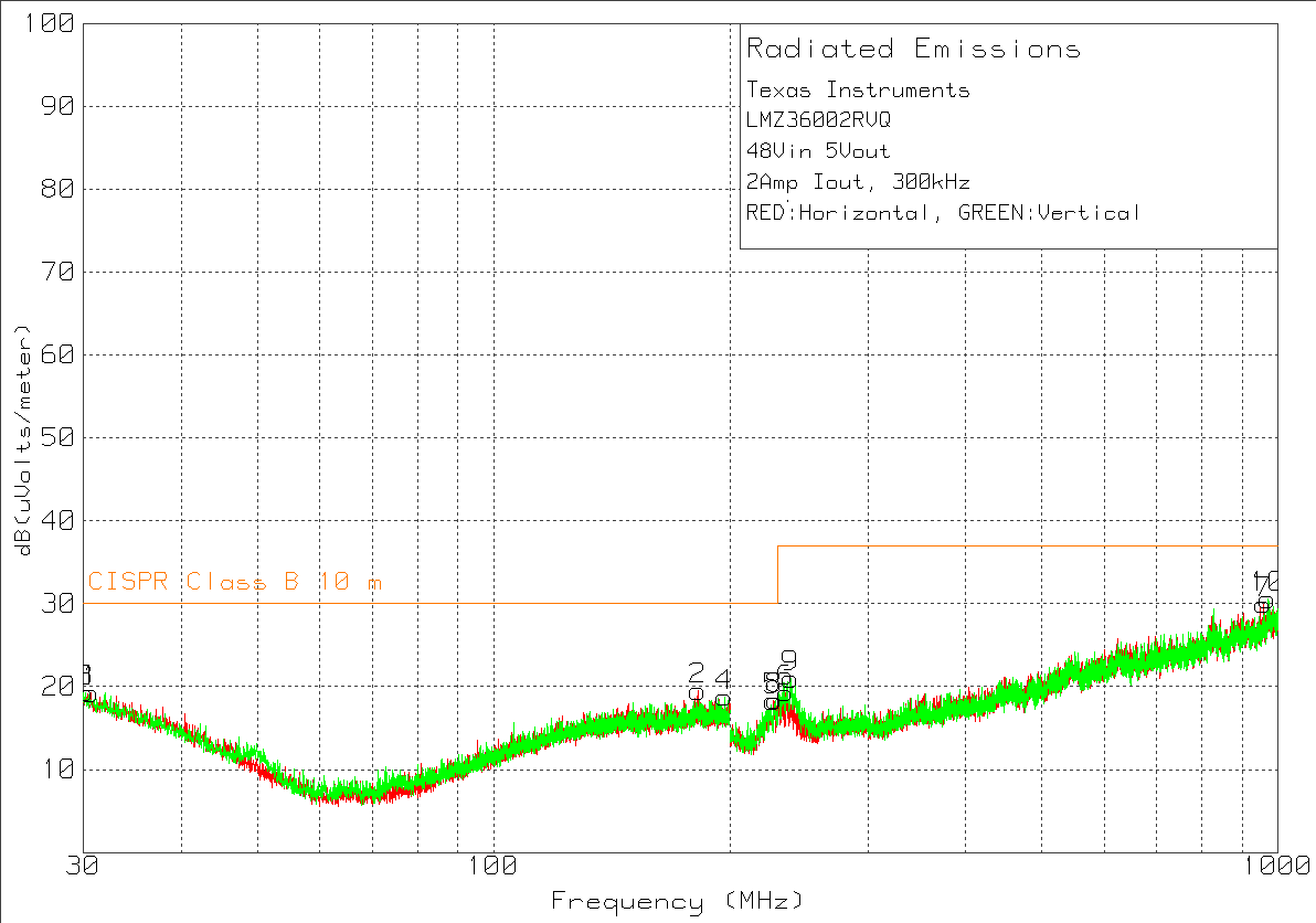
LMZ36002 EMI_48Vin_5Vout_LMZ36002.pngFigure 43. Radiated Emissions (EN55022 Class B)
48-V Input, 5-V Output, 2-A Load, 300 kHz
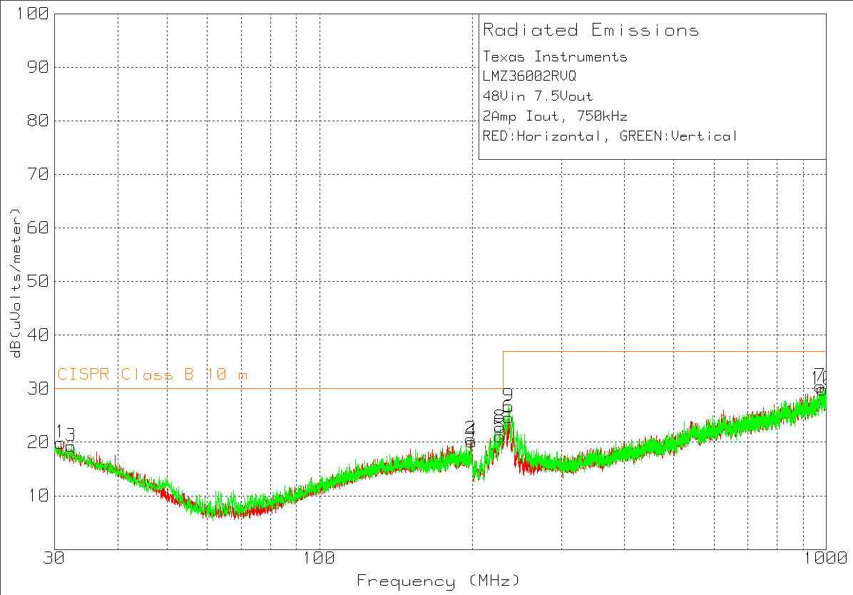
LMZ36002 EMI_48Vin_7_5Vout_LMZ36002.pngFigure 45. Radiated Emissions (EN55022 Class B)
48-V Input, 7.5-V Output, 2-A Load, 750 kHz