JAJSGE7A October 2018 – May 2019 LMZM33604
PRODUCTION DATA.
- 1 特長
- 2 アプリケーション
- 3 概要
- 4 改訂履歴
- 5 Pin Configuration and Functions
- 6 Specifications
-
7 Detailed Description
- 7.1 Overview
- 7.2 Functional Block Diagram
- 7.3
Feature Description
- 7.3.1 Adjusting the Output Voltage
- 7.3.2 Input Capacitor Selection
- 7.3.3 Output Capacitor Selection
- 7.3.4 Transient Response
- 7.3.5 Feed-Forward Capacitor
- 7.3.6 Switching Frequency (RT)
- 7.3.7 Synchronization (SYNC/MODE)
- 7.3.8 Output Enable (EN)
- 7.3.9 Programmable System UVLO (EN)
- 7.3.10 Internal LDO and BIAS_SEL
- 7.3.11 Power Good (PGOOD) and Power Good Pullup (PGOOD_PU)
- 7.3.12 Mode Select (Auto or FPWM)
- 7.3.13 Soft Start and Voltage Tracking
- 7.3.14 Voltage Dropout
- 7.3.15 Overcurrent Protection (OCP)
- 7.3.16 Thermal Shutdown
- 7.4 Device Functional Modes
- 8 Application and Implementation
- 9 Power Supply Recommendations
- 10Layout
- 11デバイスおよびドキュメントのサポート
- 12メカニカル、パッケージ、および注文情報
パッケージ・オプション
デバイスごとのパッケージ図は、PDF版データシートをご参照ください。
メカニカル・データ(パッケージ|ピン)
- RLX|41
サーマルパッド・メカニカル・データ
発注情報
7.3.10 Internal LDO and BIAS_SEL
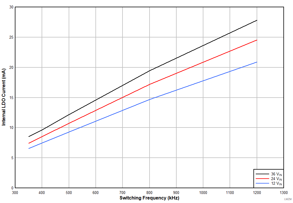
The LMZM33604 integrates an internal LDO, generating a typical VCC voltage (3.27 V) for control circuitry and MOSFET drivers. The LDO generates VCC voltage from VIN unless a sufficient bias voltage, VBIAS, is applied to BIAS_SEL pin. The BIAS_SEL input provides an option to supply the LDO with a lower voltage than VIN to reduce the LDO power loss. The smaller the difference between the input applied to the LDO, VIN_LDO, and the LDO output voltage, VCC, the more efficiently the device will perform. The amount of current supplied through the LDO will change based on operating conditions. Figure 36 demonstrates the typical LDO current, ILDO, for common input voltages over the recommended switching frequency range.

| VOUT = 5 V |
The amount of power loss in the LDO can be calculated by Equation 4.

For example, when the device is operating at VIN = 24 V, VOUT = 5 V, fsw = 500 kHz, BIAS_SEL = PGND, the ILDO is typical 11 mA, therefore, the PLOSS_LDO = 11 mA × (24 V – 3.27 V) = 228.03 mW. For the same operating conditions with BIAS_SEL = 5 V, the power loss is equal to 11 mA × (5 V – 3.27 V) = 19.03 mW. The benefits of applying a bias voltage to reduce power loss are most notable in applications when VIN » VCC or when the device is operating at a higher switching frequency. The power savings can be calculated by Equation 5.

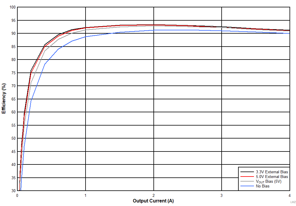
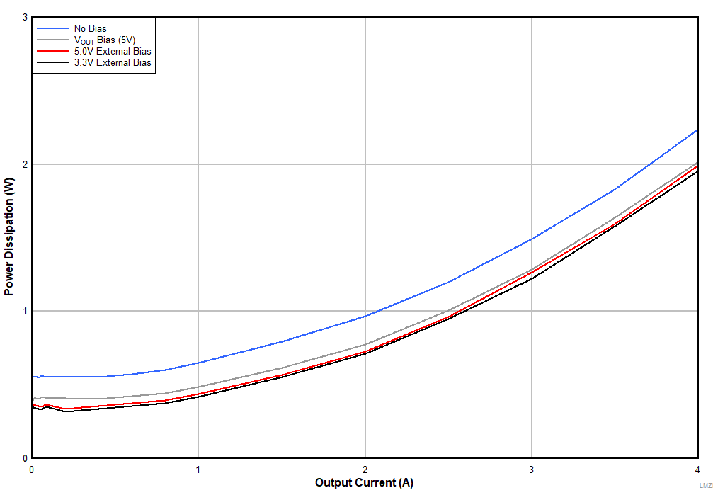
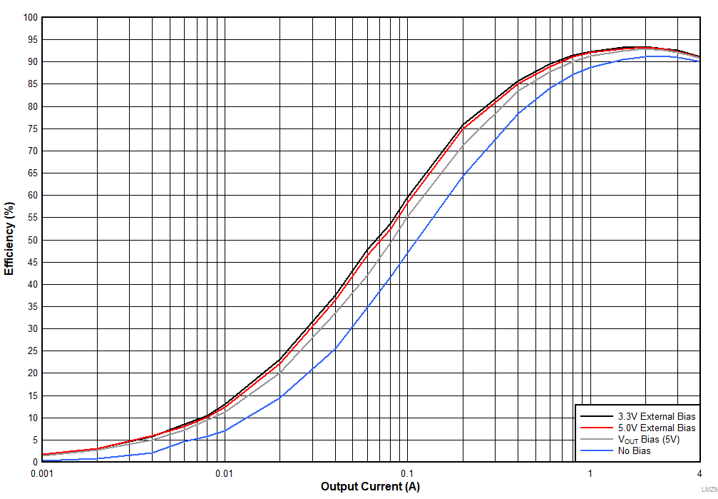
Figure 37 and Figure 38 show efficiency plots of the LMZM33604 operating with different source voltages applied to the BIAS_SEL pin. Figure 39 demonstrates the power dissipation of the device with various source voltages at BIAS_SEL pin. The plots include BIAS_SEL tied to a 3.3 V external bias, 5 V external bias, VOUT (5 V) and no bias voltage applied. The efficiency improvements are more significant when the device is operating at light loads because the LDO loss is a higher percentage of the total loss.

| VIN = 24 V | fSW = 500 kHz | FPWM Mode |

| VIN = 24 V | fSW = 500 kHz | FPWM Mode |

| VIN = 24 V | fSW = 500 kHz | FPWM Mode |