JAJSQO6A August 2023 – December 2024 LOG200
PRODMIX
- 1
- 1 特長
- 2 アプリケーション
- 3 概要
- 4 Pin Configuration and Functions
- 5 Specifications
- 6 Detailed Description
- 7 Application and Implementation
- 8 Device and Documentation Support
- 9 Revision History
- 10Mechanical, Packaging, and Orderable Information
パッケージ・オプション
デバイスごとのパッケージ図は、PDF版データシートをご参照ください。
メカニカル・データ(パッケージ|ピン)
- RGT|16
サーマルパッド・メカニカル・データ
- RGT|16
発注情報
7.2.1.3 Application Curves
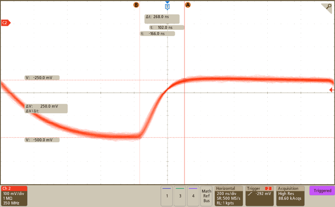
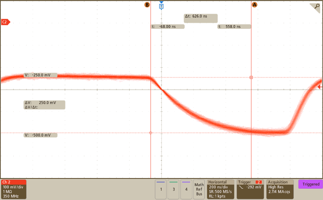
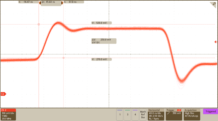
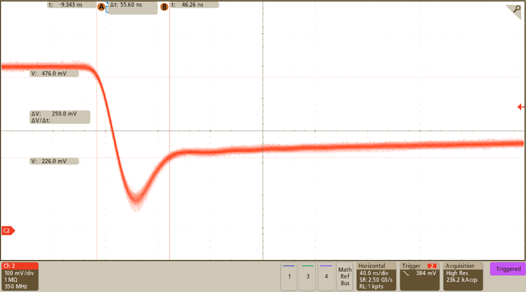
The following figures show oscilloscope captures of the LOG200 output as the device responds to one-decade shifts in the input current. Rising and falling steps between 10nA and 100nA, and between 10µA and 100µA, were recorded. The oscilloscope was set to use the ac-coupled path.
For the current steps between 10nA and 100nA, a 10mA laser diode bias was used. A rise time of approximately 268ns and a fall time of approximately 626ns are observed.
 Figure 7-6 10nA-to-100nA Current
Step
 Figure 7-7 100nA-to-10nA Current Step
For the current steps between 10µA and 100µA, a 13mA laser diode bias was used. A rise time of approximately 45.60ns and a fall time of approximately 55.60ns are observed.
 Figure 7-8 10µA-to-100µA Current
Step
 Figure 7-9 100µA-to-10µA Current
Step