JAJSPI9G June 2011 – April 2024 LP2951-Q1
PRODUCTION DATA
- 1
- 1 特長
- 2 アプリケーション
- 3 概要
- 4 Pin Configuration and Functions
- 5 Specifications
- 6 Detailed Description
- 7 Application and Implementation
- 8 Device and Documentation Support
- 9 Revision History
- 10Mechanical, Packaging, and Orderable Information
パッケージ・オプション
メカニカル・データ(パッケージ|ピン)
サーマルパッド・メカニカル・データ
- DRG|8
発注情報
7.2.2.3 CBYPASS: Noise and Stability Improvement
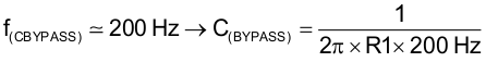
In the LP2951-Q1, an external FEEDBACK pin directly connected to the error amplifier noninverting input can allow stray capacitance to cause instability by shunting the error amplifier feedback to GND, especially at high frequencies. This instability is worsened if high-value external resistors are used to set the output voltage, because a high resistance allows the stray capacitance to play a more significant role (that is, a larger RC time delay is introduced between the output of the error amplifier and the FEEDBACK input, leading to more phase shift and lower phase margin). A solution is to add a 100-pF bypass capacitor (CBYPASS) between OUTPUT and FEEDBACK; because CBYPASS is in parallel with R1, this capacitor lowers the impedance introduced at FEEDBACK at high frequencies, in effect offsetting the effect of the parasitic capacitance by providing more feedback at higher frequencies. More feedback forces the error amplifier to work at a lower loop gain, so COUT must be increased to a minimum of 3.3 μF to improve the regulator phase margin.
CBYPASS can be also used to reduce output noise in the LP2951-Q1. This bypass capacitor reduces the closed-loop gain of the error amplifier at the high frequency, so noise no longer scales with the output voltage. This improvement is more noticeable with higher output voltages, where loop-gain reduction is greatest. An acceptable CBYPASS is calculated as shown in Equation 2: