at operating temperature TJ = 25°C,
VIN = VOUT(NOM) + 1.0 V or 2.5 V (whichever is greater),
IOUT = 1 mA, ON/OFF pin tied to VIN,
CIN = 1.0 µF, and COUT = 4.7 µF (unless otherwise
noted)
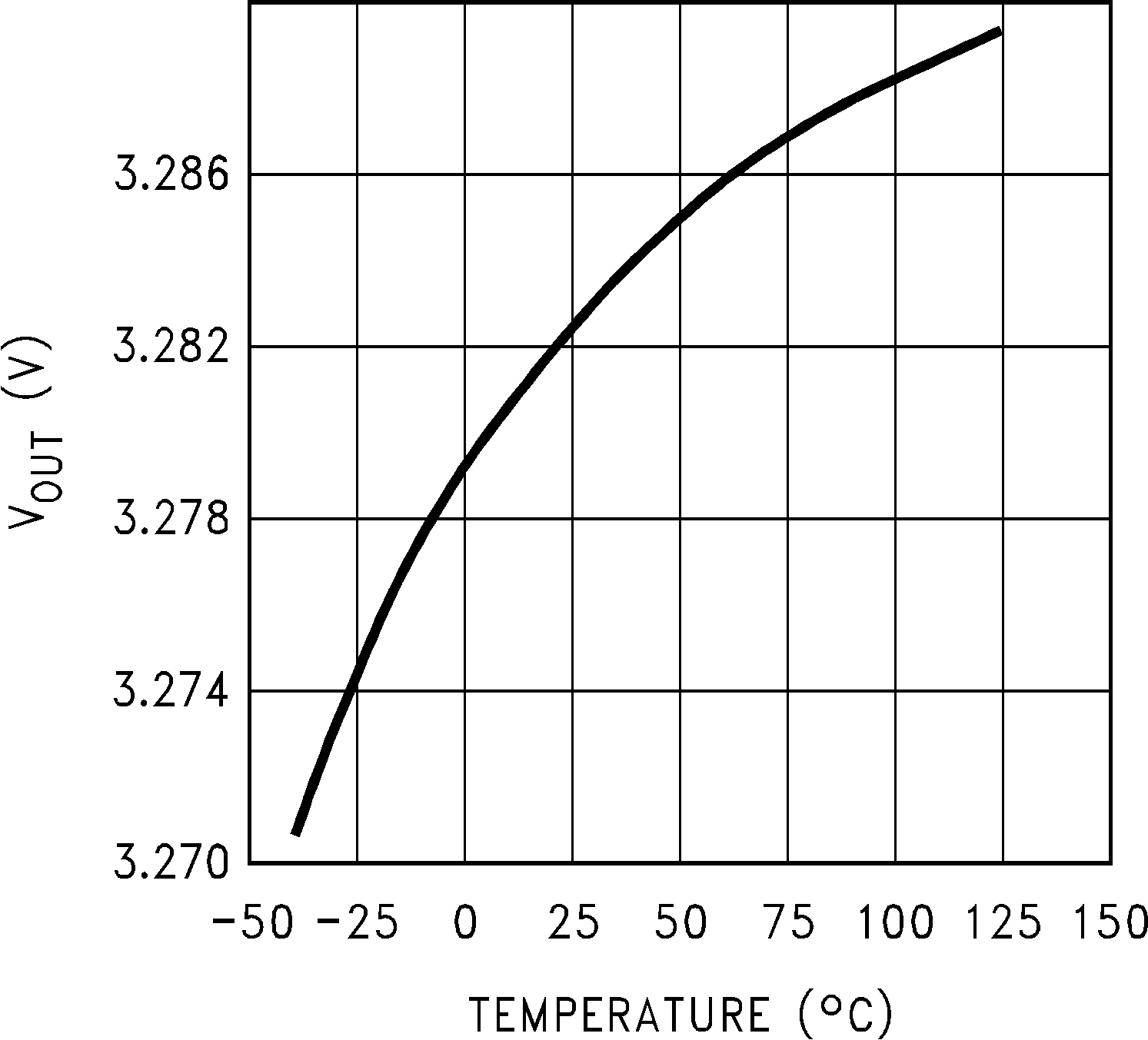
 Figure 6-1 Output Voltage vs Temperature for Legacy Chip
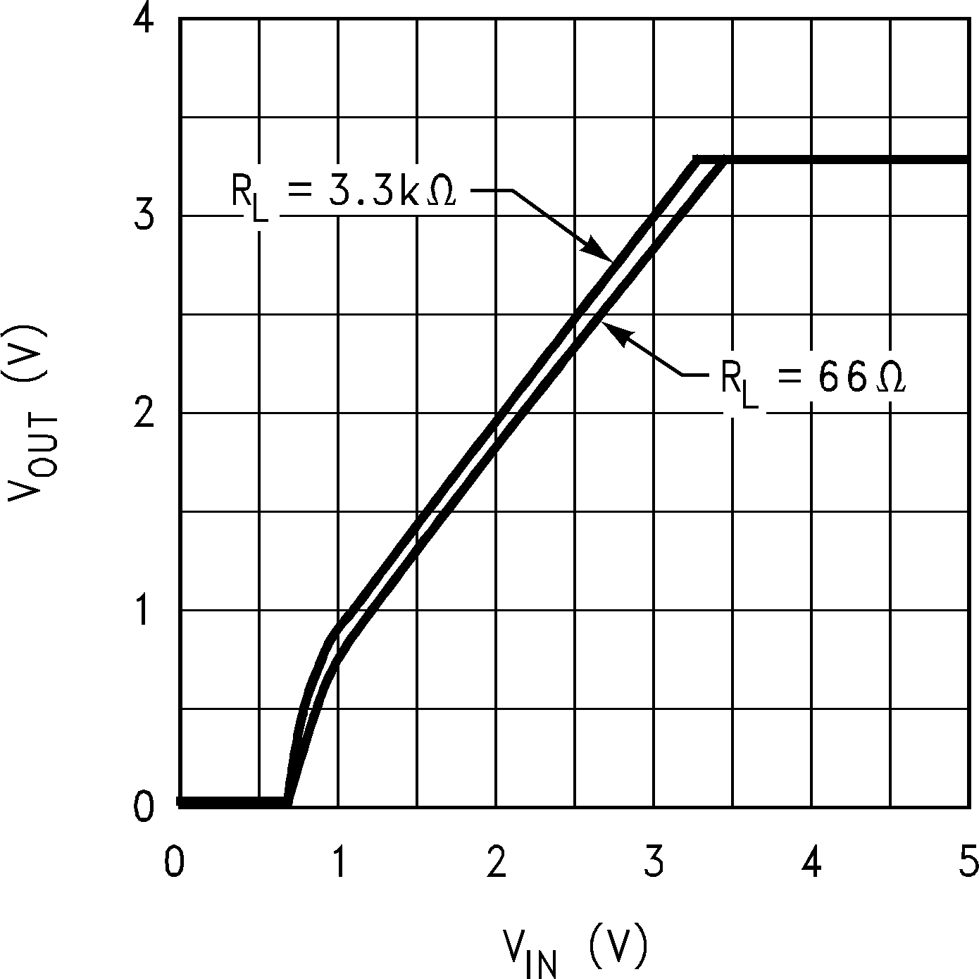
 Figure 6-3 Output Voltage vs VIN for Legacy Chip
 Figure 6-5 Dropout Voltage vs
VIN for New Chip
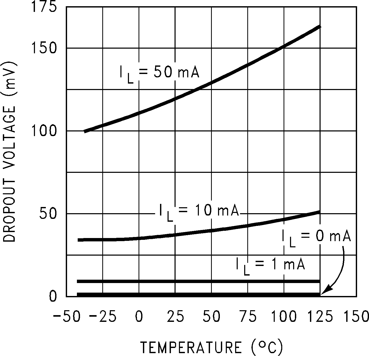
 Figure 6-7 Dropout Voltage vs Temperature for Legacy Chip
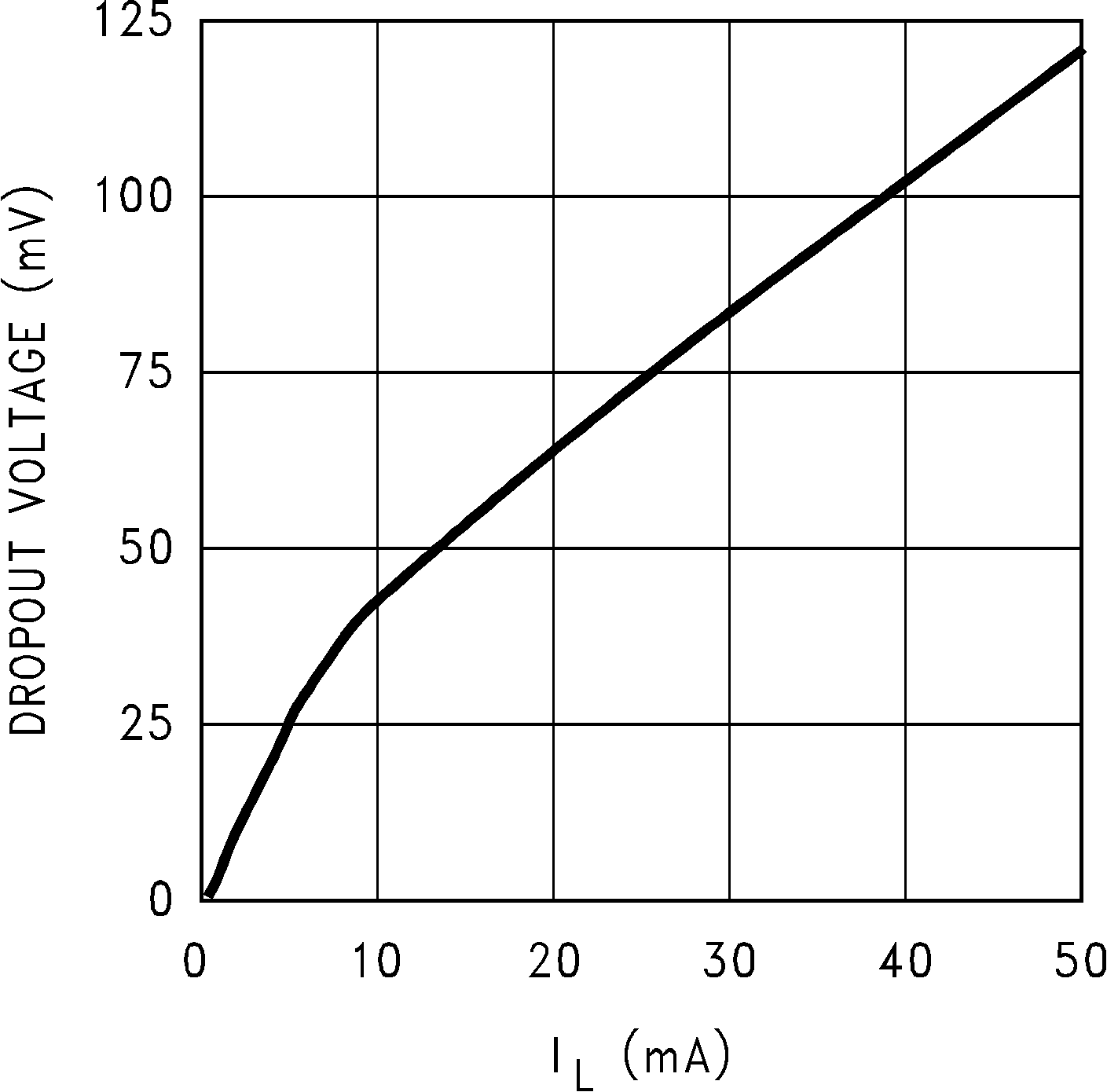
 Figure 6-9 Dropout Voltage vs Load
Current for Legacy Chip
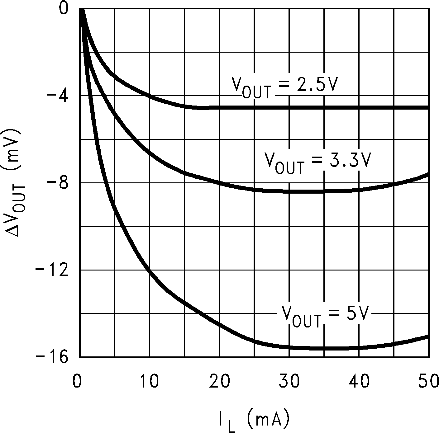
 Figure 6-11 Output Regulation vs Load
Current for Legacy Chip
 Figure 6-13 Output Regulation vs Load
Current and Temperature for New Chip
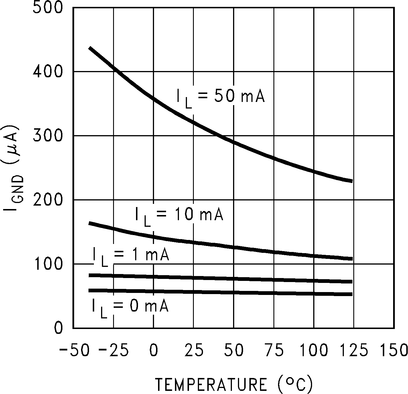
 Figure 6-15 Ground-Pin Current vs Temperature for Legacy Chip
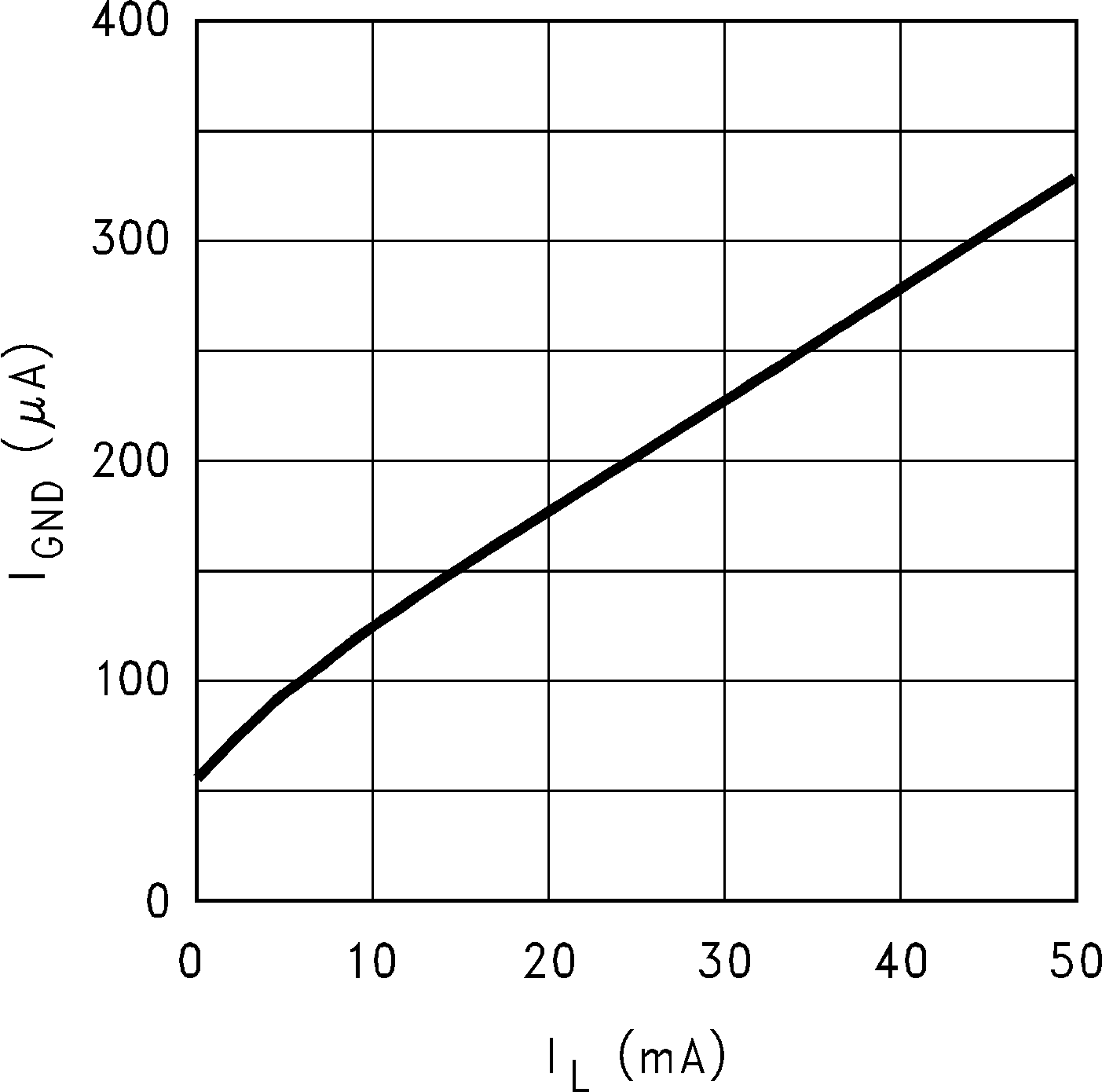
 Figure 6-17 Ground Pin Current vs Load Current for Legacy Chip
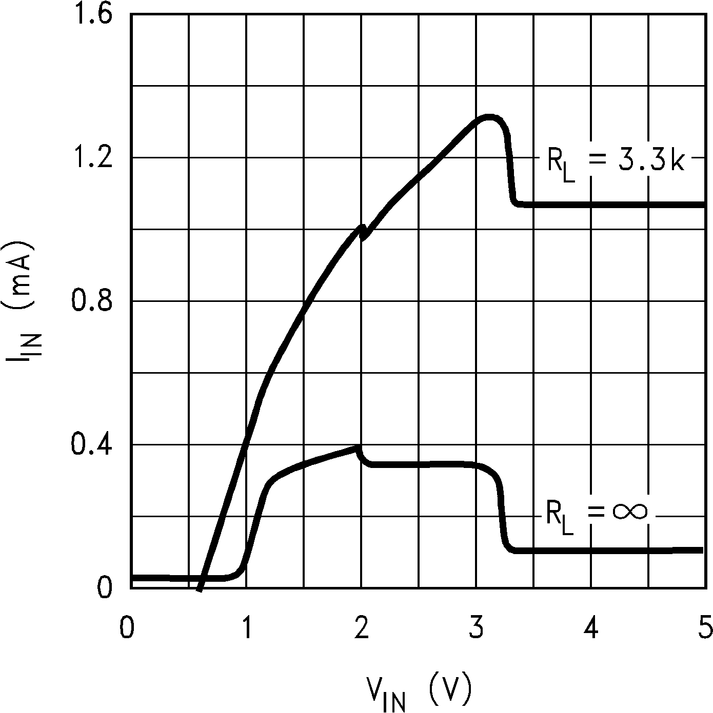
 Figure 6-19 Input
Current vs Input Voltage for Legacy Chip
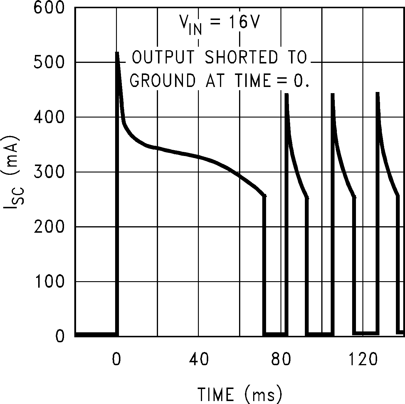
 Figure 6-21 Short-Circuit Current vs Time for Legacy Chip
 Figure 6-23 Short-Circuit Current vs Time for Legacy Chip
 Figure 6-25 Short-Circuit Current vs Output Voltage for Legacy Chip
 Figure 6-27 Short-Circuit Current vs
Temperature for New Chip
 Figure 6-29 ADJ
Pin Bias Current vs Load Current for New Chip
 Figure 6-31 ADJ
Pin Bias Current vs Temperature for New Chip
 Figure 6-33 ON/OFF Threshold vs Temperature
for New Chip
| VIN = 4.3 V, VOUT = 3.3 V,
IOUT = 50 mA, COUT = 2.2
μF |
Figure 6-35 Output Noise Density vs
CFF for New Chip
| VIN = 4.3 V, VOUT = 3.3 V,
COUT = 2.2 μF, CFF = 10
pF |
Figure 6-37 Output Noise Density vs
IOUT for New Chip
| VIN = 4.3 V, VOUT = 3.3 V,
IOUT = 50 mA, COUT = 2.2
μF |
Figure 6-39 Ripple Rejection vs CFF for New Chip
| VIN = 4.3 V, VOUT = 3.3 V,
COUT = 2.2 μF, CFF = 10
pF |
Figure 6-41 Ripple Rejection vs
IOUT for New Chip Figure 6-43 4.7-μF ESR Curves for Legacy Chip
| VIN = 4.3 V, VOUT = 3.3
V |
Figure 6-2 Output Voltage vs Temperature for New Chip Figure 6-4 Output Voltage vs
VIN for New Chip
 Figure 6-6 Dropout Voltage vs
VIN and Temperature for New Chip
 Figure 6-8 Dropout Voltage vs
Temperature for New Chip
 Figure 6-10 Dropout Voltage vs Load
Current for New Chip
 Figure 6-12 Output Regulation vs Load Current for New
Chip
 Figure 6-14 Output Regulation vs Input
Voltage for New Chip
 Figure 6-16 Ground-Pin Current vs Temperature for New Chip
 Figure 6-18 Ground Pin Current vs Load
Current for New Chip
 Figure 6-20 Input Current vs Input
Voltage for New Chip
 Figure 6-22 Short-Circuit Current vs
Time for New Chip
 Figure 6-24 Short-Circuit Current vs
Time for New Chip
 Figure 6-26 Short-Circuit Current vs
Output Voltage for New Chip
 Figure 6-28 ADJ
Pin Bias Current vs. Load Current for Legacy Chip
 Figure 6-30 ADJ
Pin Bias Current vs Temperature for Legacy Chip
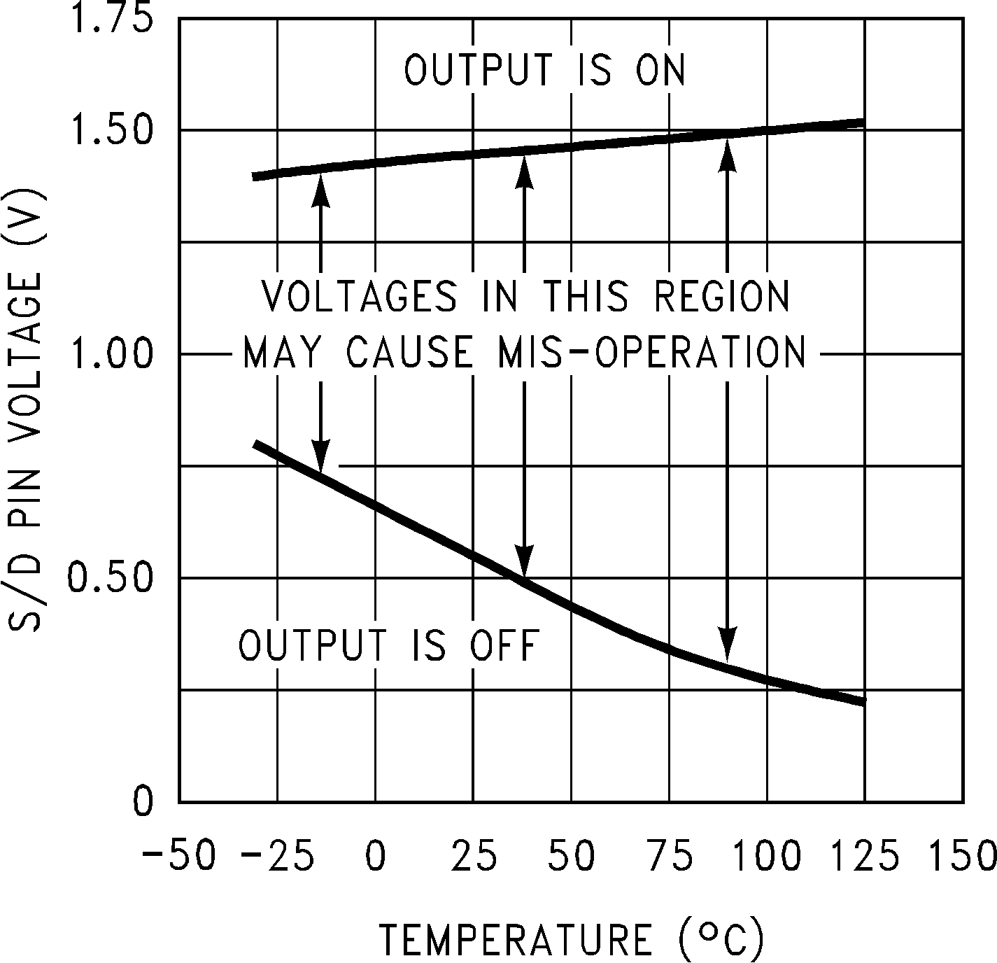
 Figure 6-32 ON/OFF Threshold vs Temperature for Legacy Chip
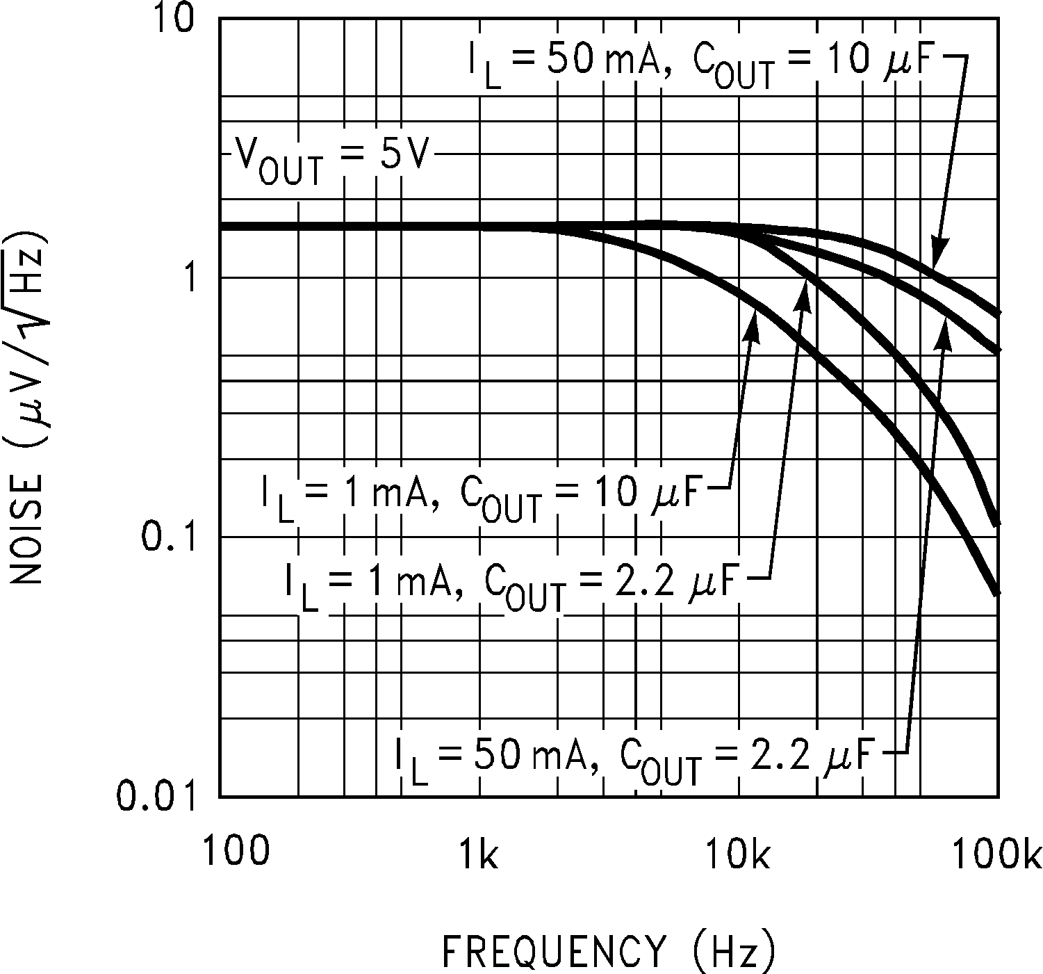
 Figure 6-34 Output Noise Density for Legacy Chip
| VIN = 4.3 V, VOUT = 3.3 V,
IOUT = 50 mA, CFF = 10
pF |
Figure 6-36 Output Noise Density vs
COUT for New Chip Figure 6-38 Ripple Rejection for Legacy Chip
| VIN = 4.3 V, VOUT = 3.3 V,
IOUT = 50 mA, CFF = 10
pF |
Figure 6-40 Ripple Rejection vs
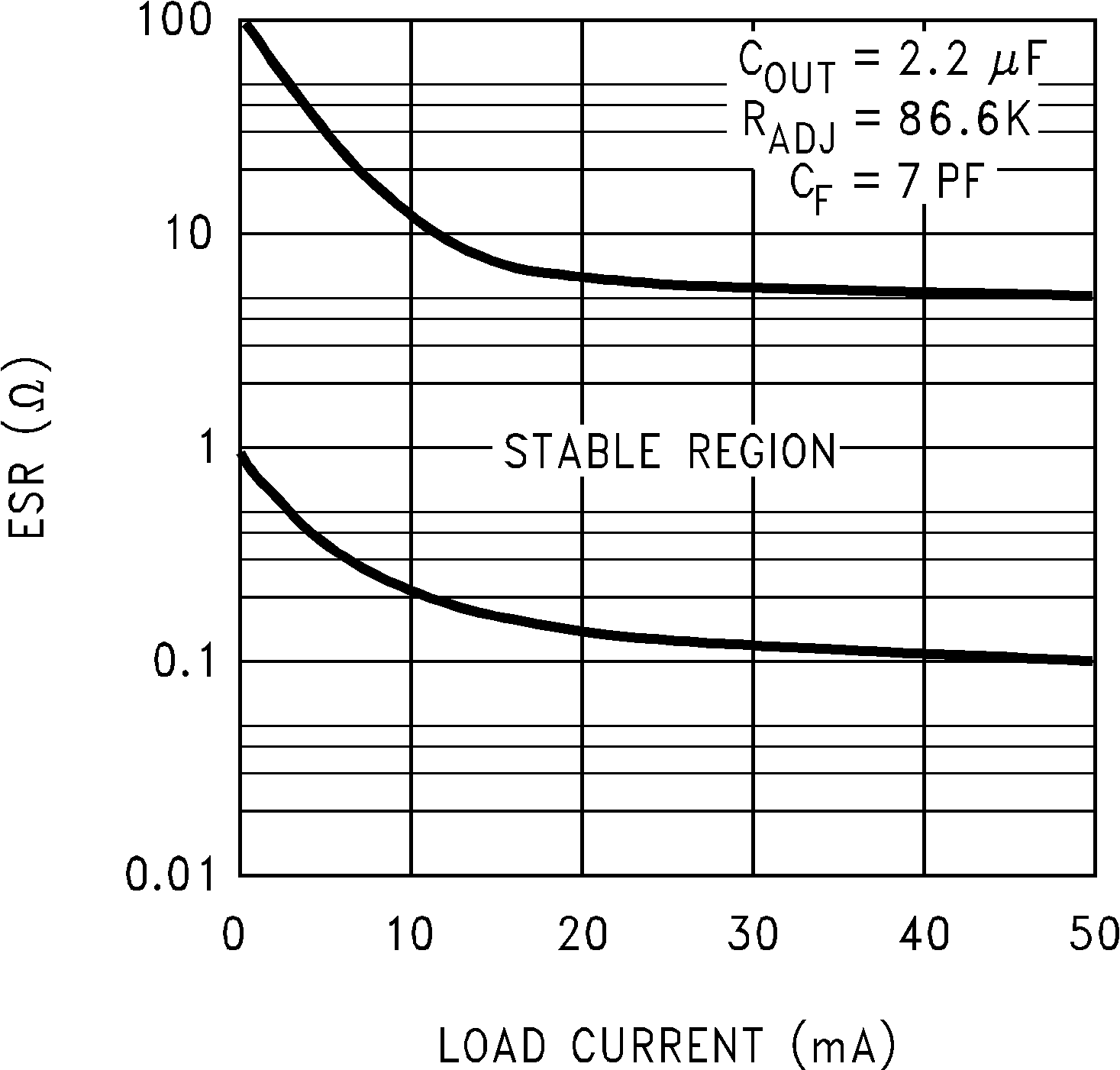
COUT for New Chip Figure 6-42 2.2-μF ESR Curves for Legacy Chip