SNVS083O February   2005  – March 2015 LP2989

PRODUCTION DATA.  

  1. Features
  2. Applications
  3. Description
  4. Revision History
  5. Pin Configuration and Functions
  6. Specifications
    1. 6.1 Absolute Maximum Ratings
    2. 6.2 ESD Ratings
    3. 6.3 Recommended Operating Conditions
    4. 6.4 Thermal Information
    5. 6.5 Electrical Characteristics
    6. 6.6 Typical Characteristics
  7. Detailed Description
    1. 7.1 Overview
    2. 7.2 Functional Block Diagram
    3. 7.3 Feature Description
      1. 7.3.1 High-Accuracy Output Voltage
      2. 7.3.2 Sleep Mode
      3. 7.3.3 Error Detection Comparator Output
      4. 7.3.4 Short Circuit Protection (Current Limit)
      5. 7.3.5 Thermal Protection
    4. 7.4 Device Functional Modes
      1. 7.4.1 Operation With 16 V ≥ VIN > VOUT(TARGET) + 1 V
      2. 7.4.2 Operation with Shutdown Control
      3. 7.4.3 Shutdown Input Operation
  8. Application and Implementation
    1. 8.1 Application Information
    2. 8.2 Typical Application
      1. 8.2.1 Design Requirements
      2. 8.2.2 Detailed Design Procedure
        1. 8.2.2.1 WSON Package Devices
        2. 8.2.2.2 External Capacitors
          1. 8.2.2.2.1 Input Capacitor
          2. 8.2.2.2.2 Output Capacitor
          3. 8.2.2.2.3 Noise Bypass Capacitor
        3. 8.2.2.3 Capacitor Characteristics
          1. 8.2.2.3.1 Ceramic
          2. 8.2.2.3.2 Tantalum
          3. 8.2.2.3.3 Film
        4. 8.2.2.4 Reverse Input-Output Voltage
      3. 8.2.3 Application Curves
  9. Power Supply Recommendations
  10. 10Layout
    1. 10.1 Layout Guidelines
    2. 10.2 Layout Example
  11. 11Device and Documentation Support
    1. 11.1 Documentation Support
      1. 11.1.1 Related Documentation
    2. 11.2 Trademarks
    3. 11.3 Electrostatic Discharge Caution
    4. 11.4 Glossary
  12. 12Mechanical, Packaging, and Orderable Information

パッケージ・オプション

メカニカル・データ(パッケージ|ピン)
サーマルパッド・メカニカル・データ
発注情報

12 Mechanical, Packaging, and Orderable Information

The following pages include mechanical, packaging, and orderable information. This information is the most current data available for the designated devices. This data is subject to change without notice and revision of this document. For browser-based versions of this data sheet, refer to the left-hand navigation.
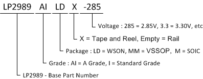
LP2989 decoder.pngFigure 45. POA Orderable Device Key