JAJSI22B July   2019  – November 2019 LP3470A

PRODUCTION DATA.  

  1. 特長
  2. アプリケーション
  3. 概要
    1.     Device Images
      1.      基本的な動作回路
      2.      LP3470A の標準的な消費電流
  4. 改訂履歴
  5. Device Comparison Table
  6. Pin Configuration and Functions
    1.     Pin Functions
  7. Specifications
    1. 7.1 Absolute Maximum Ratings
    2. 7.2 ESD Ratings
    3. 7.3 Recommended Operating Conditions
    4. 7.4 Thermal Information
    5. 7.5 Electrical Characteristics
    6. 7.6 Timing Requirements
    7. 7.7 Typical Characteristics
  8. Detailed Description
    1. 8.1 Overview
    2. 8.2 Functional Block Diagram
    3. 8.3 Feature Description
      1. 8.3.1 RESET Time-Out Period
      2. 8.3.2 RESET Output
      3. 8.3.3 Pull-up Resistor Selection
      4. 8.3.4 VCC Transient Immunity
    4. 8.4 Device Functional Modes
      1. 8.4.1 RESET Output Low
      2. 8.4.2 RESET Output High
  9. Application and Implementation
    1. 9.1 Application Information
    2. 9.2 Typical Application
      1. 9.2.1 Design Requirements
      2. 9.2.2 Detailed Design Procedure
      3. 9.2.3 Application Curves
  10. 10Power Supply Recommendations
  11. 11Layout
    1. 11.1 Layout Guidelines
    2. 11.2 Layout Example
  12. 12デバイスおよびドキュメントのサポート
    1. 12.1 ドキュメントの更新通知を受け取る方法
    2. 12.2 サポート・リソース
    3. 12.3 商標
    4. 12.4 静電気放電に関する注意事項
    5. 12.5 Glossary
  13. 13メカニカル、パッケージ、および注文情報

パッケージ・オプション

メカニカル・データ(パッケージ|ピン)
サーマルパッド・メカニカル・データ
発注情報

Application Curves

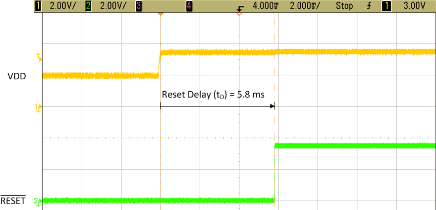
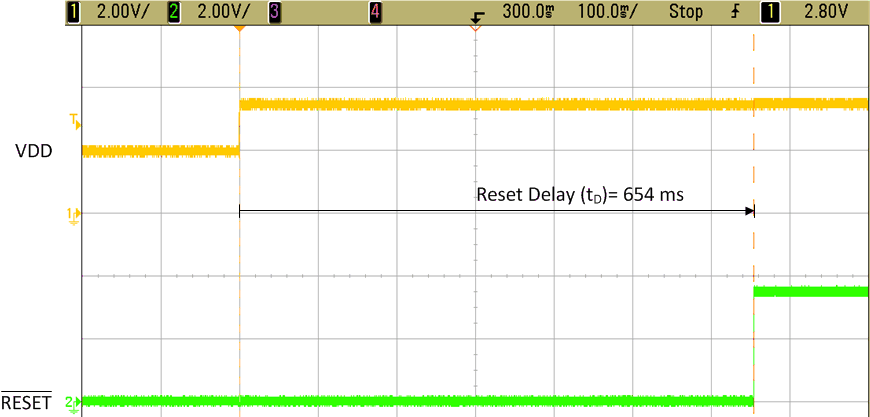
Two capacitor values for CSRT (0.1 µF and 1 µF) are used as examples to show the programmability of the output time delay as shown in Figure 12 and Figure 13.
LP3470A TPS3840_reset_delay_cap_0p01uF.gif
Figure 12. Reset Delay Time with 0.1-µF Capacitor at SRT
LP3470A TPS3840_reset_delay_cap_1uF.gif
Figure 13. Reset Delay Time with 1-µF Capacitor at SRT