SNVS522I August 2007 – August 2015 LP38501-ADJ , LP38503-ADJ
PRODUCTION DATA.
- 1 Features
- 2 Applications
- 3 Description
- 4 Revision History
- 5 Pin Configurations and Functions
- 6 Specifications
- 7 Detailed Description
- 8 Application and Implementation
- 9 Power Supply Recommendations
- 10Layout
- 11Device and Documentation Support
- 12Mechanical, Packaging, and Orderable Information
7 Detailed Description
7.1 Overview
The LP38501-ADJ and LP38503-ADJ are FlexCap and low-dropout adjustable regulators, the output voltage can be set from 0.6 V to 5 V. Standard regulator features, such as overcurrent and overtemperature protections, are also included.
The LP38501-ADJ and LP38503-ADJ contain several features:
- Stable with any type of output capacitor
- Fast load transient response
- Disable Mode (LP38501-ADJ only)
7.2 Functional Block Diagrams
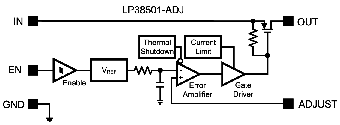 Figure 11. LP38501-ADJ Block Diagram
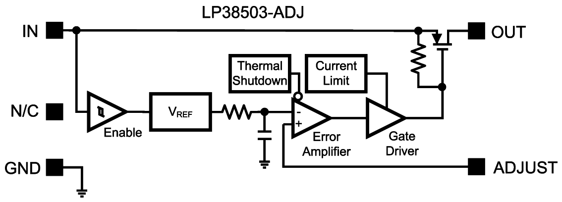 Figure 12. LP38503-ADJ Block Diagram
7.3 Feature Description
7.3.1 Stability and Phase Margin
Any regulator which operates using a feedback loop must be compensated in such a way as to ensure adequate phase margin, which is defined as the difference between the phase shift and –180 degrees at the frequency where the loop gain crosses unity (0 dB). For most LDO regulators, the ESR of the output capacitor is required to create a zero to add enough phase lead to ensure stable operation.
Figure 13 shows the gain/phase plot of the LP38501-ADJ and LP38503-ADJ with an output of 1.2 V, a 10-µF ceramic output capacitor, delivering 2 A of load current. The unity-gain crossover occurs at 300 kHz, and the phase margin is about 40° (which is very stable).
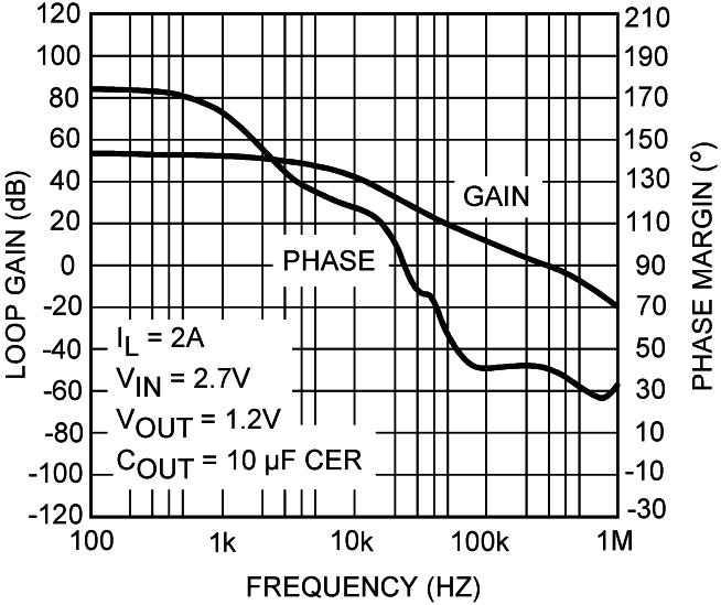 Figure 13. Gain-Bandwidth Plot for 2-A Load
Figure 14 shows the gain and phase with no external load. In this case, the only load is provided by the gain setting resistors (about 12 kΩ total in this test). It is immediately obvious that the unity-gain frequency is significantly lower (dropping to about 500 Hz), at which point the phase margin is 125°.
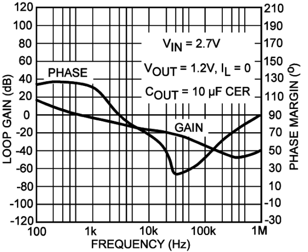 Figure 14. Gain-Bandwidth Plot for No Load
The reduction in unity-gain bandwidth as load current is reduced is normal for any LDO regulator using a P-FET or PNP pass transistor, because they have a pole in the loop gain function given by:

Equation 1 calculates how the pole goes to the highest frequency when RL is minimum value (maximum load current). In general, LDOs have maximum bandwidth (and lowest phase margin) at full load current. In the case of the LP38501-ADJ, good phase margin is seen even when using ceramic capacitors with ESR values of only a few mΩ.
7.3.2 Load Transient Response
Load transient response is defined as the change in regulated output voltage which occurs as a result of a change in load current. Many applications have loads which vary, and the control loop of the voltage regulator must adjust the current in the pass FET transistor in response to load current changes. For this reason, regulators with wider bandwidths often have better transient response.
The LP38501-ADJ employs an internal feed-forward design which makes the load transient response much faster than would be predicted simply by loop speed; this feedforward means any voltage changes appearing on the output are coupled through to the high-speed driver used to control the gate of the pass FET along a signal path using very fast FET devices. Because of this, the pass transistor’s current can change very quickly.
Figure 15 shows the output transient response resulting from a change in load current of 0.1 A – 3 A, and then 3 A – 0.1 A with a load current slew rate of 500 mA/µs. As shown in Figure 15, the resulting change in output voltage is only about 40 mV (peak), which is just slightly over 2% for the 1.8-V output used for this test. This is excellent performance for such a small output capacitor.
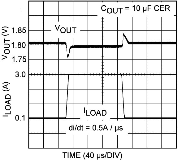 Figure 15. Load Transient Response: 10-µF Ceramic, 0.5-A/µs Di/Dt
When the load current changes much more quickly, the output voltage will show more change because the loop and internal feedforward circuitry are not able to react as fast as the load changes. In such cases, it is the output capacitor which must supply load current during the transition until the loop responds and changes the pass transistor’s drive to deliver the new value of load current. As an example, the slew rate of the load current will be increased to 75 A/μs and the same test will be performed. In Figure 16, it can be seen that the peak excursion of the output voltage during the transient has now increased to about 200 mV, which is just slightly over 11% for the 1.8-V output.
 Figure 16. Load Transient Response: 10-μF Ceramic, 75 A/μs di/dt
A better understanding of the load transient can be obtained when the load’s rising edge is expanded in time scale (Figure 16).
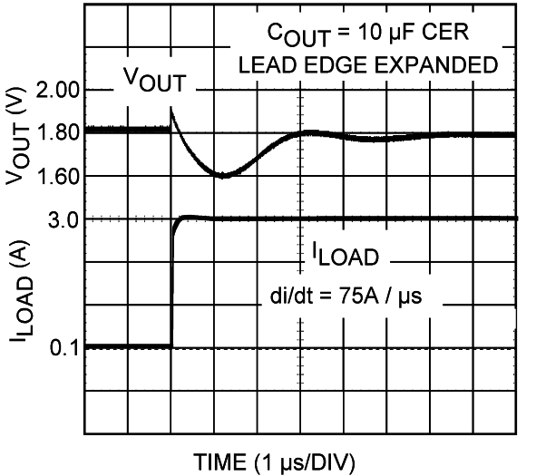 Figure 17. Rising Edge, 10-µF Ceramic, 75 A/µs di/dt
Figure 16 shows that the output voltage starts “correcting” back upwards after less than a microsecond, and has fully reversed direction after about 1.2 µs. This very rapid reaction is a result of the maximum loop bandwidth (full load is being delivered) and the feedforward effect kicking on the drive to the FET before feedback gets fully around the loop.
In cases where extremely fast load changes occur, and output voltage regulation better than 10% is required, the output capacitance must be increased. When selecting capacitors, it must be understood that the better performing ones usually cost the most. For fast changing loads, the internal parasitics of ESR (equivalent series resistance) and ESL (equivalent series inductance) degrade the capacitor’s ability to source current quickly to the load. The best capacitor types for transient performance are (in order):
- Multilayer Ceramic: with the lowest values of ESR and ESL, they can have ESR values in the range of a few milli Ohms. Disadvantage: capacitance values above about 22 µF significantly increase in cost.
- Low-ESR Aluminum Electrolytics: these are aluminum types (like OSCON) with a special electrolyte which provides extremely low ESR values, and are the closest to ceramic performance while still providing large amounts of capacitance. These are cheaper (by capacitance) than ceramic.
- Solid tantalum: can provide several hundred µF of capacitance, transient performance is slightly worse than OSCON type capacitors, cheaper than ceramic in large values.
- General purpose aluminum electrolytics: cheap and provide a lot of capacitance, but give the worst performance.
As a first example, larger values of ceramic capacitance show how much reduction can be obtained from the 200-mV output change (Figure 16) which was seen with only a 10-µF ceramic output capacitor. In Figure 18, the 10-µF output capacitor is increased to 22 µF. The 200-mV transient is reduced to about 160 mV, which is from about 11% of VOUT down to about 9%.
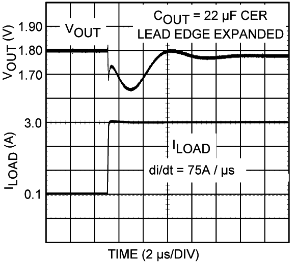 Figure 18. 22-µF Ceramic Output Capacitor
In Figure 19, the output capacitance is increased to 47 µF ceramic. It can be seen that the output transient is further reduced down to about 120 mV, which is still about 6.6% of the output voltage. This shows that a 5X increase in ceramic capacitance from the original 10 µF only reduced the peak voltage transient amplitude by about 40%.
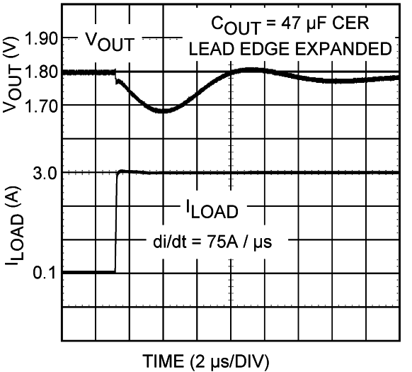 Figure 19. 47-µF Ceramic Output Capacitor
In general, managing load transients is done by paralleling ceramic capacitance with a larger bulk capacitance. In this way, the ceramic can source current during the rapidly changing edge and the bulk capacitor can support the load current after the first initial spike in current.
In the next test, the same 10-µF ceramic capacitor is paralleled with a general-purpose (less expensive) aluminum electrolytic whose capacitance is 220 µF. As shown in Figure 20, there is a small improvement over the 200 mV peak seen with the 10-µF ceramic capacitor alone. By adding the 220 µF aluminum capacitor, the peak is reduced to about 160 mV (the same peak value as seen with a 22-µF ceramic capacitor alone).
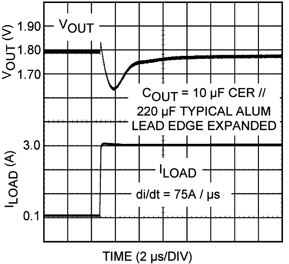 Figure 20. 10-µF Ceramic Paralleled by 220-µF Generic Aluminum Electrolytic
A solid Tantalum works better, so the aluminum electrolytic is replaced by a 220-µF Tantalum (Figure 21). The peak amplitude of the output transient is now reduced to about 130 mV, just slightly less efficient than the value of the 47-µF ceramic capacitor alone.
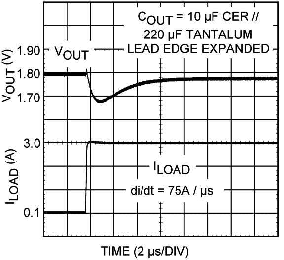 Figure 21. 10-µF Ceramic Paralleled by 220-µF Tantalum
The OSCON (ultra low ESR) aluminum electrolytic is the best of the electrolytics. Figure 22 shows the output voltage transient is reduced down to about 90 mV (about 5% of VOUT) when a 220-µF OSCON is added to the 10 µF ceramic. This indicates that some kind of ultra-low ESR aluminum electrolytic used in parallel with some ceramic capacitance is probably the best approach for extremely fast transients, but each application must be dialed in for it’s specific load requirements.
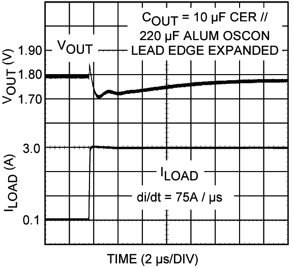 Figure 22. 10-µF Ceramic Paralleled by 220-µF OSCON
7.3.3 Dropout Voltage
The dropout voltage of a regulator is defined as the input-to-output differential required by the regulator to keep the output voltage within 2% of the nominal value. For CMOS LDOs, the dropout voltage is the product of the load current and the RDS(on) of the internal MOSFET pass element.
Because the output voltage is beginning to “drop out” of regulation when it drops by 2%, electrical performance of the device is reduced compared to the values listed in Electrical Characteristics for some parameters (line and load regulation and PSRR would be affected).
7.3.4 Reverse Current Path
The internal MOSFET pass element in the LP38501-ADJ and LP38503-ADJ has an inherent parasitic diode. During normal operation, the input voltage is higher than the output voltage and the parasitic diode is reverse biased. However, if the output is pulled above the input in an application, then current flows from the output to the input as the parasitic diode gets forward biased. The output can be pulled above the input as long as the current in the parasitic diode is limited to 200-mA continuous and 1-A peak. The regulator output pin must not be taken below ground potential. If the LP38501-ADJ and LP38503-ADJ is used in a dual-supply system where the regulator load is returned to a negative supply, the output must be diode-clamped to ground.
7.3.5 Short-Circuit Protection
The LP38501-ADJ and LP38503-ADJ contain internal current limiting which reduces output current to a safe value if the output is overloaded or shorted. Depending upon the value of VIN, thermal limiting may also become active as the average power dissipated causes the die temperature to increase to the limit value (about 170°C). The hysteresis of the thermal shutdown circuitry can result in a “cyclic” behavior on the output as the die temperature heats and cools.
7.4 Device Functional Modes
7.4.1 Enable Operation (LP38501-ADJ Only)
The ENABLE pin (EN) must be actively terminated by either a 10-kΩ pullup resistor to VIN, or a driver which actively pulls high and low (such as a CMOS rail to rail comparator). If active drive is used, the pullup resistor is not required. This pin must be tied to VIN if not used (it must not be left floating).