SNVS522I August 2007 – August 2015 LP38501-ADJ , LP38503-ADJ
PRODUCTION DATA.
- 1 Features
- 2 Applications
- 3 Description
- 4 Revision History
- 5 Pin Configurations and Functions
- 6 Specifications
- 7 Detailed Description
- 8 Application and Implementation
- 9 Power Supply Recommendations
- 10Layout
- 11Device and Documentation Support
- 12Mechanical, Packaging, and Orderable Information
10 Layout
10.1 Layout Guidelines
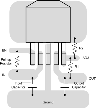
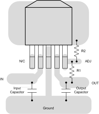
Good layout practices minimize voltage error and prevent instability which can result from ground loops. The input and output capacitors must be directly connected to the device pins with short traces that have no other current flowing in them (Kelvin connect).
The best way to do this is to place the capacitors very near the device and make connections directly to the device pins via short traces on the top layer of the PCB. The regulator ground pin must be connected through vias to the internal or backside ground plane so that the regulator has a single point ground.
The external resistors which set the output voltage must also be located very near the device with all connections directly tied via short traces to the pins of the device (Kelvin connect). Do not connect the resistive divider to the load point or DC error could be induced.
10.2 Layout Examples
 Figure 29. LP38501-ADJ TO-263 Layout
 Figure 30. LP38503-ADJ TO-263 Layout