SNVS522I August 2007 – August 2015 LP38501-ADJ , LP38503-ADJ
PRODUCTION DATA.
- 1 Features
- 2 Applications
- 3 Description
- 4 Revision History
- 5 Pin Configurations and Functions
- 6 Specifications
- 7 Detailed Description
- 8 Application and Implementation
- 9 Power Supply Recommendations
- 10Layout
- 11Device and Documentation Support
- 12Mechanical, Packaging, and Orderable Information
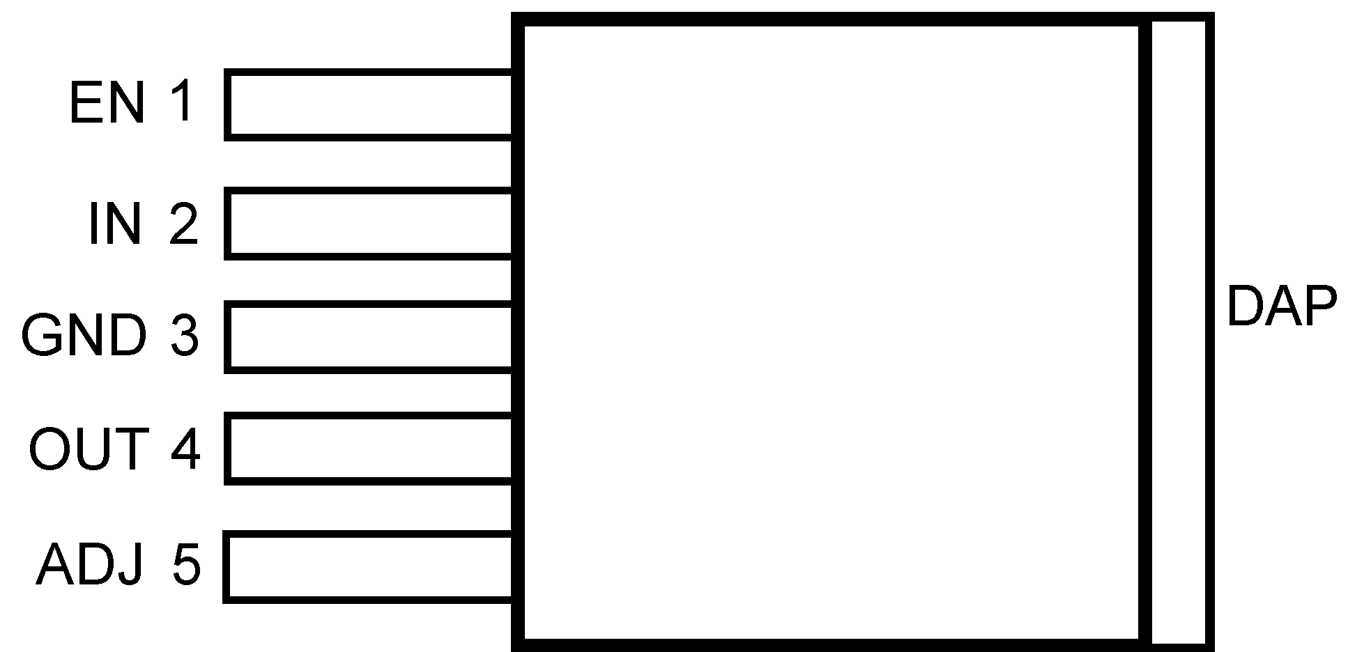
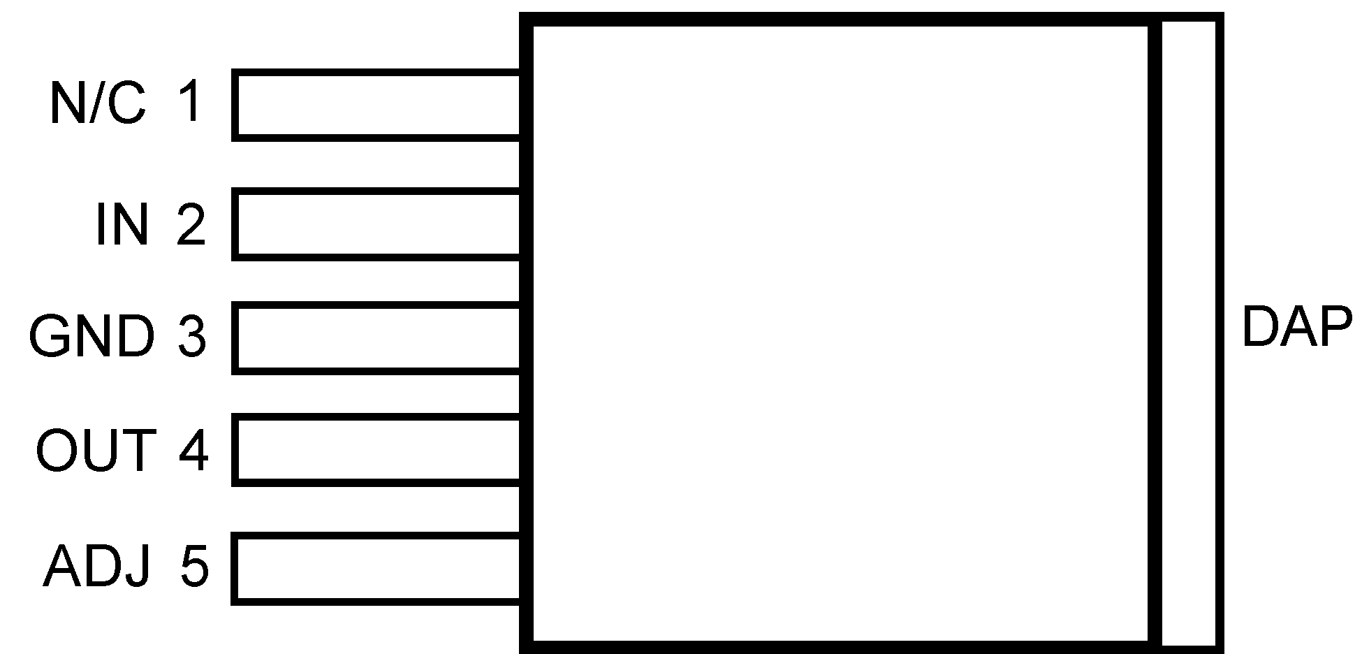
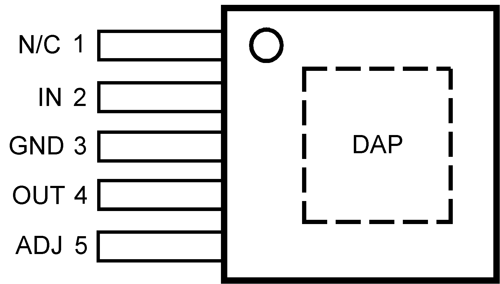
5 Pin Configurations and Functions
KTT Package (LP38501)
5-Pin DDPAK/TO-263
Top View

KTT Package (LP38503)
5-Pin DDPAK/TO-263
Top View

NDQ Package (LP38501)
5-Pin TO-263
Top View

NDQ Package (LP38503)
5-Pin TO-263
Top View

Pin Functions
| PIN | TYPE | DESCRIPTION | ||||
|---|---|---|---|---|---|---|
| LP38501 | LP38503 | LP38501 | LP38503 | |||
| NAME | DDPAK/TO-263 | TO-263 | ||||
| ADJ | 5 | 5 | 5 | 5 | O | Sets output voltage. |
| EN | 1 | — | 1 | — | I | Enable (LP38501-ADJ only). Pull high to enable the output, low to disable the output. This pin has no internal bias and must be either tied to the input voltage, or actively driven. |
| GND | 3 | 3 | 3 | 3 | G | Ground |
| IN | 2 | 2 | 2 | 2 | I | Input supply pin. |
| N/C | — | 1 | — | 1 | — | In the LP38503-ADJ, this pin has no internal connections. It can be left floating or used for trace routing. |
| OUT | 4 | 4 | 4 | 4 | O | Regulated output voltage pin. |
| DAP | √ | √ | √ | √ | — | The DAP is used as a thermal connection to remove heat from the device to the circuit board DAP copper clad area which acts as the heatsink. The DAP is electrically connected to the backside of the die. The DAP must be connected to ground potential, but can not be used as the only ground connection. |