-
LP3869x-ADJ/Q1 500-mA Low-Dropout CMOS Linear Regulators Stable With Ceramic Output Capacitors SNVS324K January 2005 – January 2016 LP38691-ADJ , LP38691-ADJ-Q1 , LP38693-ADJ , LP38693-ADJ-Q1
PRODUCTION DATA.
-
LP3869x-ADJ/Q1 500-mA Low-Dropout CMOS Linear Regulators Stable With Ceramic Output Capacitors
- 1 Features
- 2 Applications
- 3 Description
- 4 Revision History
- 5 Pin Configuration and Functions
- 6 Specifications
- 7 Detailed Description
-
8 Application and Implementation
- 8.1 Application Information
- 8.2
Typical Applications
- 8.2.1 Design Requirements
- 8.2.2 Detailed Design Procedure
- 8.2.3 Application Curve
- 9 Power Supply Recommendations
- 10Layout
- 11Device and Documentation Support
- 12Mechanical, Packaging, and Orderable Information
- IMPORTANT NOTICE
LP3869x-ADJ/Q1 500-mA Low-Dropout CMOS Linear Regulators Stable With Ceramic Output Capacitors
1 Features
- Wide Input Voltage Range: 2.7 V to 10 V
- All WSON Options are Available as AEC-Q100 Grade 1
- Output Voltage Range: 1.25 V to 9 V
- 2% Adjust (ADJ) Pin Voltage Accuracy (25°C)
- Low Dropout Voltage: 250 mV at 500 mA
(Typical, 5-V Out) - Precision (Trimmed) Bandgap Reference
- Ensured Specs for –40°C to +125°C
- 1-µA Off-State Quiescent Current
- Thermal Overload Protection
- Foldback Current Limiting
- Ground (GND) Pin Current: 55 µA (Typical) at Full Load
- Enable (EN) Pin (LP38693-ADJ)
2 Applications
- Hard Disk Drives
- Notebook Computers
- Battery-Powered Devices
- Portable Instrumentation
3 Description
The LP3869x-ADJ low-dropout CMOS linear regulators provide 2% precision reference voltage, extremely low dropout voltage (250 mV at 500-mA load current, VOUT = 5 V), and excellent AC performance using ultra-low equivalent series resistance (ESR) ceramic output capacitors.
The low thermal resistance of the WSON and SOT-223 packages allow use of the full operating current even in high ambient temperature environments.
The use of a PMOS power transistor means that no DC base drive current is required to bias it, thus allowing the GND-pin current to remain below 100 µA regardless of load current, input voltage, or operating temperature.
Device Information(1)
| PART NUMBER | PACKAGE | BODY SIZE (NOM) |
|---|---|---|
| LP38691-ADJ | WSON (6) | 3.00 mm × 3.00 mm |
| LP38693-ADJ | SOT-223 (5) | 6.50 mm × 3.56 mm |
| WSON (6) | 3.00 mm × 3.00 mm |
- For all available packages, see the orderable addendum at the end of the data sheet.
Typical Application Circuits


4 Revision History
Changes from J Revision (October 2015) to K Revision
- Added Caution note to Foldback Current Limiting subsection Go
Changes from I Revision (April 2013) to J Revision
- Added Device Information and Pin Configuration and Functions sections, ESD Ratings table, update Thermal Values; add Feature Description, Device Functional Modes, Application and Implementation, Power Supply Recommendations, Layout, Device and Documentation Support, and Mechanical, Packaging, and Orderable Information sections; update Vin, Vout and Ven pin names to IN, OUT, and EN in text and graphics; modified wording of Description to eliminate redundancy; added top nav icon for reference design.Go
Changes from H Revision (April 2013) to I Revision
5 Pin Configuration and Functions
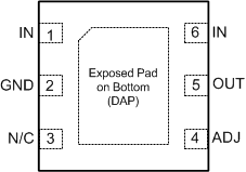
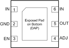
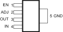
Pin Functions
| PIN | I/O | DESCRIPTION | |||
|---|---|---|---|---|---|
| LP38691-ADJ | LP38693-ADJ | ||||
| NAME | WSON | WSON | SOT-223 | ||
| DAP | √ | √ | — | — | WSON Only - The DAP (exposed pad) functions as a thermal connection when soldered to a copper plane. See WSON Mounting section for more information. |
| EN | — | 3 | 1 | I | The EN pin allows the part to be turned to an ON or OFF state by pulling this pin high or low. |
| GND | 2 | 2 | 5 | — | Circuit ground for the regulator. For the SOT-223 package this is thermally connected to the die and functions as a heat sink when the soldered down to a large copper plane. |
| IN | 1, 6 | 1, 6 | 4 | I | This is the input supply voltage to the regulator. For WSON devices, both IN pins must be tied together for full current operation (250 mA maximum per pin). |
| N/C | 3 | — | — | — | No internal connection. |
| ADJ | 4 | 4 | 2 | O | The ADJ pin is used to set the regulated output voltage by connecting it to the external resistors R1 and R2 (see Typical Application Circuits). |
| OUT | 5 | 5 | 3 | I | Regulated output voltage. |
6 Specifications
6.1 Absolute Maximum Ratings
over operating free-air temperature range (unless otherwise noted)(1)(2)| MIN | MAX | UNIT | ||
|---|---|---|---|---|
| V(MAX) All pins (with respect to GND) | –0.3 | 12 | V | |
| IOUT(4) | Internally limited | V | ||
| Power dissipation(3) | Internally limited | V | ||
| Junction temperature | –40 | 150 | °C | |
| Storage temperature, Tstg | −65 | 150 | ||
6.2 ESD Ratings: LP38691-ADJ, LP38693-ADJ
| VALUE | UNIT | |||
|---|---|---|---|---|
| V(ESD) | Electrostatic discharge | Human-body model (HBM), per ANSI/ESDA/JEDEC JS-001(1) | ±2000 | V |
6.3 ESD Ratings: LP38691-ADJ-Q1, LP38693-ADJ-Q1
| VALUE | UNIT | |||
|---|---|---|---|---|
| V(ESD) | Electrostatic discharge | Human-body model (HBM), per AEC Q100-002(1) | 2000 | V |
6.4 Recommended Operating Conditions
| MIN | NOM | MAX | UNIT | ||
|---|---|---|---|---|---|
| VIN supply voltage | 2.7 | 10 | V | ||
| Operating junction temperature | −40 | 125 | °C | ||
6.5 Thermal Information
| THERMAL METRIC(1) | LP3869x-ADJ | LP38693-ADJ | UNIT | |
|---|---|---|---|---|
| WSON | SOT-223 | |||
| 6 PINS | 5 PINS | |||
| RθJA(2) | Junction-to-ambient thermal resistance, High-K | 50.6 | 68.5(3) | °C/W |
| RθJC(top) | Junction-to-case (top) thermal resistance | 44.4 | 52.2 | |
| RθJB | Junction-to-board thermal resistance | 24.9 | 13.0 | |
| ψJT | Junction-to-top characterization parameter | 0.4 | 5.5 | |
| ψJB | Junction-to-board characterization parameter | 25.1 | 12.8 | |
| RθJC(bot) | Junction-to-case (bottom) thermal resistance | 5.4 | n/a | |
6.6 Electrical Characteristics
Unless otherwise specified, limits apply for TJ = 25°C, VIN = VOUT + 1 V, CIN = COUT = 10 µF, ILOAD = 10 mA. Minimum and maximum limits are specified through testing, statistical correlation, or design.| PARAMETER | TEST CONDITIONS | MIN | TYP(1) | MAX | UNIT | ||
|---|---|---|---|---|---|---|---|
| VADJ | ADJ pin voltage | VIN = 2.7 V | 1.225 | 1.25 | 1.275 | V | |
| 3.2 V ≤ VIN ≤ 10 V, 100 µA < IL < 0.5 A | 1.25 | ||||||
| 3.2 V ≤ VIN ≤ 10 V, 100 µA < IL < 0.5 A Full operating temperature range |
1.2 | 1.3 | |||||
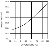
| ΔVOUT/ΔVIN | Output voltage line regulation(2) | VOUT + 0.5 V ≤ VIN ≤ 10 V IL = 25 mA |
0.03 | %/V | |||
| VOUT + 0.5 V ≤ VIN ≤ 10 V IL = 25 mA Full operating temperature range |
0.1 | ||||||
| ΔVOUT/ΔIL | Output voltage load regulation(3) | 1 mA < IL < 0.5 A VIN = VOUT + 1 V |
1.8 | %/A | |||
| 1 mA < IL < 0.5 A VIN = VOUT + 1 V Full operating temperature range |
5 | ||||||
| VDO | Dropout voltage(4) | (VOUT = 2.5 V) | IL = 0.1 A | 80 | mV | ||
| IL = 0.5 A | 430 | ||||||
| (VOUT = 2.5 V) Full operating temperature range |
IL = 0.1 A | 145 | |||||
| IL = 0.5 A | 725 | ||||||
| (VOUT = 3.3 V) | IL = 0.1 A | 65 | |||||
| IL = 0.5 A | 330 | ||||||
| (VOUT = 3.3 V) Full operating temperature range |
IL = 0.1 A | 110 | |||||
| IL = 0.5 A | 550 | ||||||
| (VOUT = 5 V) | IL = 0.1 A | 45 | |||||
| IL = 0.5 A | 250 | ||||||
| (VOUT = 5 V) Full operating temperature range |
IL = 0.1 A | 100 | |||||
| IL = 0.5 A | 450 | ||||||
| IQ | Quiescent current | VIN ≤ 10 V, IL =100 µA – 0.5 A | 55 | µA | |||
| VIN ≤ 10 V, IL =100 µA – 0.5 A Full operating temperature range |
100 | ||||||
| VEN ≤ 0.4 V, (LP38693 Only) | 0.001 | 1 | |||||
| IL(MIN) | Minimum load current | VIN – VOUT ≤ 4 V Full operating temperature range |
100 | ||||
| IFB | Foldback current limit | VIN – VOUT > 5 V | 350 | mA | |||
| VIN – VOUT < 4 V | 850 | ||||||
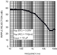
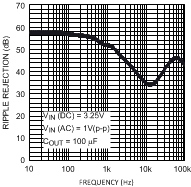
| PSRR | Ripple rejection | VIN = VOUT + 2 V(DC), with 1 V(p-p) / 120-Hz Ripple | 55 | dB | |||
| TSD | Thermal shutdown activation (junction temp) | 160 | °C | ||||
| TSD (HYST) | Thermal shutdown hysteresis (junction temp) | 10 | |||||
| IADJ | ADJ input leakage current | VADJ = 0 V to 1.5 V, VIN = 10 V | –100 | 0.01 | 100 | nA | |
| en | Output noise | BW = 10 Hz to 10 kHz VOUT = 3.3 V |
0.7 | µV/√Hz | |||
| VOUT (LEAK) | Output leakage current | VOUT = VOUT(NOM) + 1 V at 10 VIN | 0.5 | 2 | µA | ||
| VEN | Enable voltage (LP38693 Only) | Output = OFF state Full operating temperature range |
0.4 | V | |||
| Output = ON state, VIN = 4 V Full operating temperature range |
1.8 | ||||||
| Output = ON state, VIN = 6 V Full operating temperature range |
3 | ||||||
| Output = ON state, VIN = 10 V Full operating temperature range |
4 | ||||||
| IEN | EN pin leakage (LP38693 only) |
VEN = 0 V or 10 V, VIN = 10 V | –1 | 0.001 | 1 | µA | |
6.7 Typical Characteristics
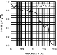
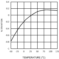
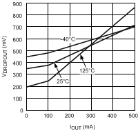
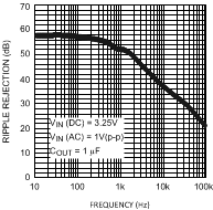
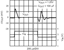
Unless otherwise specified: TJ = 25°C, CIN = COUT = 10 µF, EN pin is tied to IN (LP38693-ADJ only), VOUT = 1.25 V, VIN = VOUT 1 V, ILOAD = 10 mA.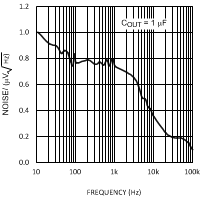
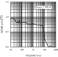 Figure 3. Noise vs Frequency
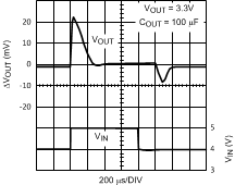
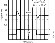
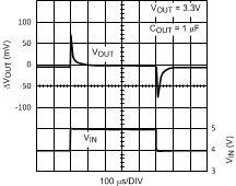
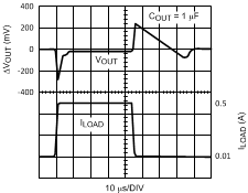
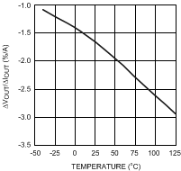
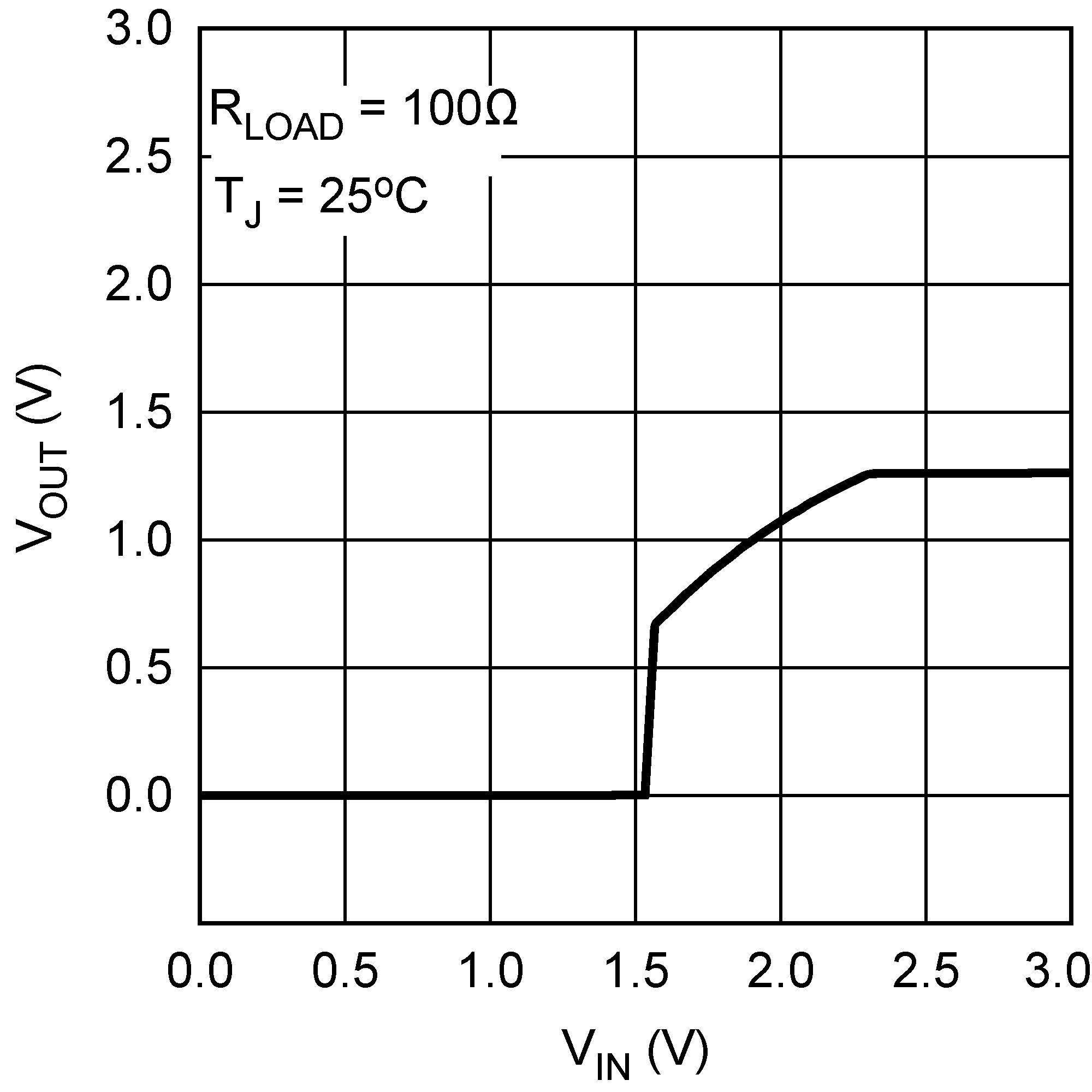
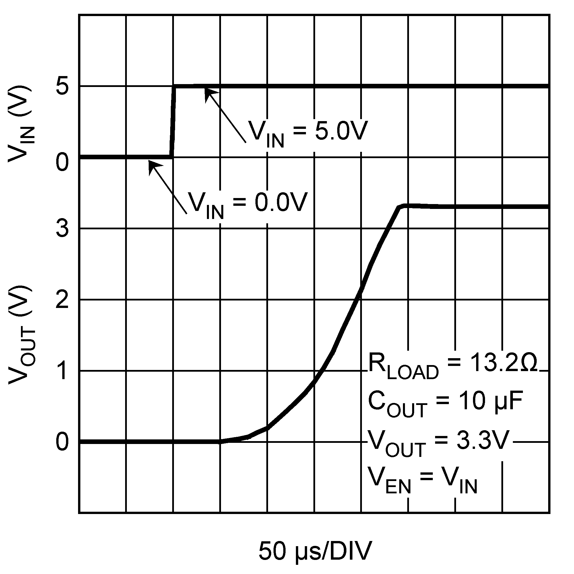
| VOUT = 1.25 V |
| VOUT = 1.8 V |
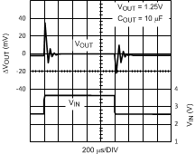
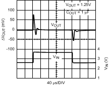
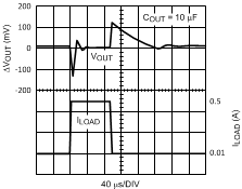
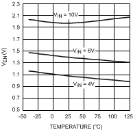
| VOUT = 1.8 V |
7 Detailed Description
7.1 Overview
The LP3869x-ADJ devices are designed to meet the requirements of portable, battery-powered digital systems providing an accurate output voltage with fast start-up. When disabled via a low logic signal at the enable pin (EN), the power consumption is reduced to virtually zero (LP38693-ADJ only).
These LP3869x-ADJ devices perform well with a single 1-μF input capacitor and a single 1-μF ceramic output capacitor.
7.2 Functional Block Diagrams
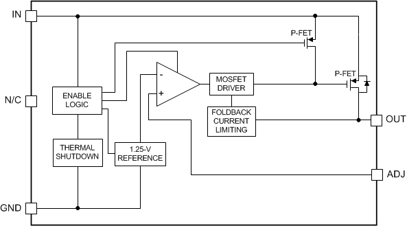 Figure 26. LP38691 Functional Diagram (WSON)
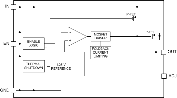 Figure 27. LP38693 Functional Diagram (SOT-223, WSON)
7.3 Feature Description
7.3.1 Enable (EN)
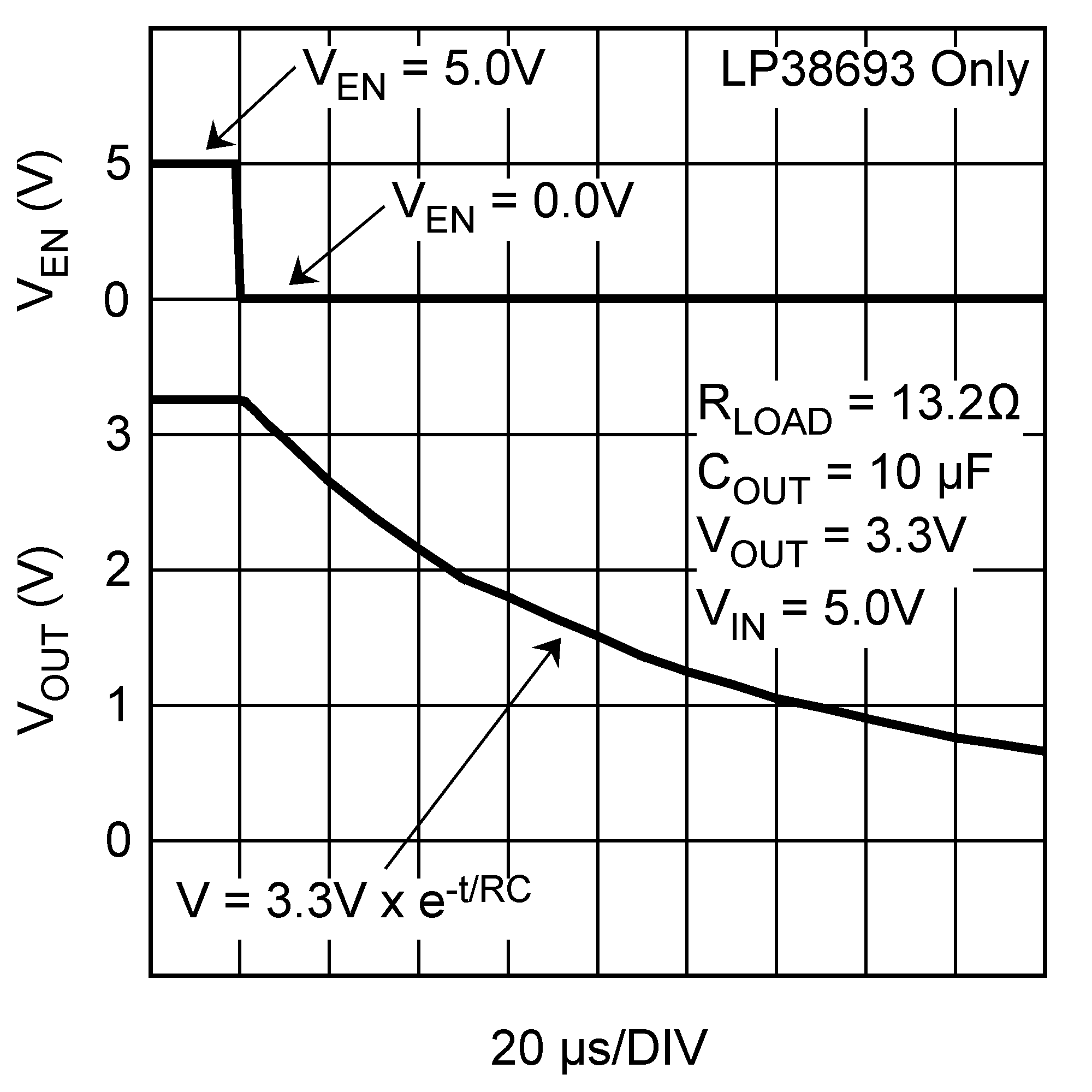
The LP38693-ADJ has an enable pin (EN) which allows an external control signal to turn the regulator output to either an ON or OFF state. The Enable on/off threshold has no hysteresis. The voltage signal must rise and fall cleanly, and promptly, through the on and off voltage thresholds. The EN pin voltage must be higher than the VEN(MIN) threshold to ensure that the device is fully enabled under all operating conditions. The EN pin voltage must be lower than the VEN(MAX) threshold to ensure that the device is fully disabled. The EN pin has no internal pullup or pulldown to establish a default condition and, as a result, this pin must be terminated either actively or passively. If the EN pin is driven from a source that actively pulls high and low, the drive voltage should not be allowed to go below ground potential or higher than VIN. If the application does not require the enable function, the EN pin should be connected directly to the IN pin.
7.3.2 Thermal Overload Protection (TSD)
Thermal shutdown disables the output when the junction temperature rises to approximately 160°C which allows the device to cool. When the junction temperature cools to approximately 150°C, the output circuitry enables.
Based on power dissipation, thermal resistance, and ambient temperature, the thermal protection circuit may cycle on and off. This thermal cycling limits the dissipation of the regulator and protects it from damage as a result of overheating. The TSD circuitry of the LP38693 has been designed to protect against temporary thermal overload conditions.
The TSD circuitry was not intended to replace proper heat-sinking. Continuously running the LP38693 device into thermal shutdown degrades device reliability.
7.3.3 Foldback Current Limiting
Foldback current limiting is built into the LP3869x-ADJ devices which reduces the amount of output current the part can deliver as the output voltage is reduced. The amount of load current is dependent on the differential voltage between the VIN and VOUT. Typically, when this differential voltage exceeds 5 V, the load current will limit at about 350 mA. When the VIN – VOUT differential is reduced below 4 V, load current is limited to about 850 mA.
CAUTION
When toggling the LP38693 Enable (EN) after the input voltage (VIN) is applied, the foldback current limit circuitry is functional the first time that the EN pin is taken high. The foldback current limit circuitry is non-functional the second, and subsequent, times that the EN pin is taken high. Depending on the input and output capacitance values the input inrush current may be higher than expected which can cause the input voltage to droop.
If the EN pin is connected to the IN pin, the foldback current limit circuitry is functional when VIN is applied if VIN starts from less than 0.4 V.
7.4 Device Functional Modes
7.4.1 Enable (EN)
The LP38693-ADJ may be switched to the ON or OFF state by logic input at the EN pin. A logic-high voltage on the EN pin turns the device to the ON state. A logic-low voltage on the EN pin turns the device to the OFF state. If the application does not require the shutdown feature, the EN pin must be tied to VIN to keep the regulator output permanently in the ON state when power is applied.
To ensure proper operation, the signal source used to drive the EN input must be able to swing above and below the specified turnon or turnoff voltage thresholds listed in the Electrical Characteristics section under VEN.