SNVS322M December 2004 – December 2015 LP38690 , LP38692
PRODUCTION DATA.
- 1 Features
- 2 Applications
- 3 Description
- 4 Revision History
- 5 Pin Configuration and Functions
- 6 Specifications
- 7 Detailed Description
- 8 Application and Implementation
- 9 Power Supply Recommendations
- 10Layout
- 11Device and Documentation Support
- 12Mechanical, Packaging, and Orderable Information
5 Pin Configuration and Functions
LP38690 TO-252 (NDP)
3 Pins
Top View

LP38690 WSON (NGG)
6 Pins
Top View

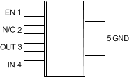
LP38690/92 SOT-223 (NDC)
5 Pins
Top View

LP38692 WSON (NGG)
6 Pins
Top View

Pin Functions
| PIN | TYPE | DESCRIPTION | ||||
|---|---|---|---|---|---|---|
| NAME | LP38690 | LP38692 | ||||
| TO-252 | WSON | SOT-223 | WSON | |||
| EN | — | — | 1 | 3 | I | The Enable (EN) pin allows the part to be turned ON and OFF by pulling this pin HIGH or LOW. |
| GND | TAB | 2 | 5 | 2 | — | Circuit ground for the regulator. For the TO-252 and SOT-223 packages this is thermally connected to the die and functions as a heat sink when soldered down to a large copper plane. |
| IN | 3 | 1, 6 | 4 | 1, 6 | I | This is the input supply voltage to the regulator. For WSON devices, both IN pins must be tied together for full current operation (500 mA maximum per pin). |
| OUT | 1 | 4 | 3 | 4 | O | Regulated output voltage. |
| SNS | — | 5 | — | 5 | I | WSON only - Output sense pin allows remote sensing at the load which eliminates the error in output voltage due to voltage drops caused by the resistance in the traces between the regulator and the load. This pin must be tied to VOUT. |
| DAP | — | X | — | X | — | WSON only - The DAP (Exposed Pad) functions as a thermal connection when soldered to a copper plane. See WSON Mounting section in Layout for more information. |