JAJSEE0C December 2014 – January 2018 LP3907-Q1
PRODUCTION DATA.
- 1 特長
- 2 アプリケーション
- 3 概要
- 4 改訂履歴
- 5 デバイス比較表
- 6 Pin Configuration and Functions
-
7 Specifications
- 7.1 Absolute Maximum Ratings
- 7.2 ESD Ratings
- 7.3 Recommended Operating Conditions (Bucks)
- 7.4 Thermal Information
- 7.5 General Electrical Characteristics
- 7.6 Low Dropout Regulators, LDO1 And LDO2
- 7.7 Buck Converters SW1, SW2
- 7.8 I/O Electrical Characteristics
- 7.9 Power-On Reset (POR) Threshold/Function
- 7.10 I2C Interface Timing Requirements
- 7.11 Typical Characteristics — LDO
- 7.12 Typical Characteristics — Bucks
- 7.13 Typical Characteristics — Buck1
- 7.14 Typical Characteristics — Buck2
- 7.15 Typical Characteristics — Bucks
-
8 Detailed Description
- 8.1 Overview
- 8.2 Functional Block Diagram
- 8.3
Feature Description
- 8.3.1 DC-DC Converters
- 8.3.2
SW1, SW2: Synchronous Step-Down Magnetic DC-DC Converters
- 8.3.2.1 Functional Description
- 8.3.2.2 Circuit Operation Description
- 8.3.2.3 PWM Operation
- 8.3.2.4 Internal Synchronous Rectification
- 8.3.2.5 Current Limiting
- 8.3.2.6 PFM Operation
- 8.3.2.7 SW1, SW2 Operation
- 8.3.2.8 SW1, SW2 Control Registers
- 8.3.2.9 Soft Start
- 8.3.2.10 Low Dropout Operation
- 8.3.2.11 Flexible Power Sequencing of Multiple Power Supplies
- 8.3.2.12 Power-Up Sequencing Using the EN_T Function
- 8.3.3 Flexible Power-On Reset (Power Good with Delay)
- 8.3.4 Undervoltage Lockout
- 8.4 Device Functional Modes
- 8.5 Programming
- 8.6
Register Maps
- 8.6.1
LP3907-Q1 Control Registers
- 8.6.1.1 Interrupt Status Register (ISRA) 0x02
- 8.6.1.2 Control 1 Register (SCR1) 0x07
- 8.6.1.3 EN_DLY Preset Delay Sequence After EN_T Assertion
- 8.6.1.4 Buck and LDO Output Voltage Enable Register (BKLDOEN) – 0x10
- 8.6.1.5 Buck and LDO Status Register (BKLDOSR) – 0x11
- 8.6.1.6 Buck Voltage Change Control Register 1 (VCCR) – 0x20
- 8.6.1.7 Buck1 Target Voltage 1 Register (B1TV1) – 0x23
- 8.6.1.8 Buck1 Target Voltage 2 Register (B1TV2) – 0x24
- 8.6.1.9 Buck1 Ramp Control Register (B1RC) - 0x25
- 8.6.1.10 Buck2 Target Voltage 1 Register (B2TV1) – 0x29
- 8.6.1.11 Buck2 Target Voltage 2 Register (B2TV2) – 0x2A
- 8.6.1.12 Buck2 Ramp Control Register (B2RC) - 0x2B
- 8.6.1.13 Buck Function Register (BFCR) – 0x38
- 8.6.1.14 LDO1 Control Register (LDO1VCR) – 0x39
- 8.6.1.15 LDO2 Control Register (LDO2VCR) – 0x3A
- 8.6.1
LP3907-Q1 Control Registers
- 9 Application and Implementation
- 10Power Supply Recommendations
- 11Layout
- 12デバイスおよびドキュメントのサポート
- 13メカニカル、パッケージ、および注文情報
パッケージ・オプション
メカニカル・データ(パッケージ|ピン)
サーマルパッド・メカニカル・データ
- RTW|24
発注情報
8.3.2.12 Power-Up Sequencing Using the EN_T Function
EN_T assertion causes the LP3907-Q1 to emerge from Standby mode to Full Operation mode at a preset timing sequence. By default, the enables for the LDOs and Bucks (ENLDO1, ENLDO2, EN_T, ENSW1, ENSW2) are 500 KΩ internally pulled down, which causes the part to stay OFF until enabled. If the user wishes to use the preset timing sequence to power on the regulators, transition the EN_T pin from Low to High. Otherwise, simply tie the enables of each specific regulator HIGH to turn on automatically.
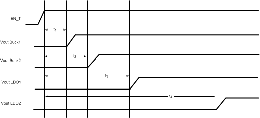
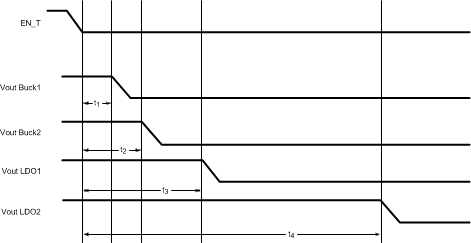
EN_T is edge triggered with rising edge signaling the chip to power on. The EN_T input is deglitched, and the default is set at 1 ms. As shown in Figure 32 and Figure 33, a rising EN_T edge starts a power-on sequence, while a falling EN_T edge starts a shutdown sequence. If EN_T is high, toggling the external enables of the regulators has no effect on the chip.
The regulators can also be programmed through I2C to turn on and off. By default, I2C enables for the regulators turned ON.
The regulators are on following the pattern below:
Regulators on = (I2C enable) AND (External pin enable OR EN_T high).
NOTE
The EN_T power-up sequencing may also be employed immediately after VIN is applied to the device. However, VIN must be stable for approximately 8 ms minimum before EN_T be asserted high to ensure internal bias, reference, and the Flexible POR timing are stabilized. This initial EN_T delay is necessary only upon first time device power on for power sequencing function to operate properly. If the device is powered, the EN_T logic must be stable for 12 ms minimum before switching state.
 Figure 32. Power Rail Enable Logic
 Figure 33. LP3907-Q1 Default Power-Up Sequence
Table 5. Power-On Timing Specification
| DESCRIPTION | MIN | NOM | TYP | UNIT | |
|---|---|---|---|---|---|
| t1 | Programmable delay from EN_T assertion to VCC_Buck1 On | 1.5 | ms | ||
| t2 | Programmable delay from EN_T assertion to VCC_Buck2 On | 2 | ms | ||
| t3 | Programmable delay from EN_T assertion to VCC_LDO1 On | 3 | ms | ||
| t4 | Programmable delay from EN_T assertion to VCC_LDO2 On | 6 | ms |
 Figure 34. LP3907-Q1 Default Power-Off Sequence
Table 6. Power-Off Timing Specification
| DESCRIPTION | MIN | NOM | MAX | UNIT | |
|---|---|---|---|---|---|
| t1 | Programmable delay from EN_T deassertion to VCC_Buck1 Off | 1.5 | ms | ||
| t2 | Programmable delay from EN_T deassertion to VCC_Buck2 Off | 2 | ms | ||
| t3 | Programmable delay from EN_T deassertion to VCC_LDO1 Off | 3 | ms | ||
| t4 | Programmable delay from EN_T deassertion to VCC_LDO2 Off | 6 | ms |