SNVS468L September 2006 – November 2015 LP3972
PRODUCTION DATA.
- 1 Features
- 2 Applications
- 3 Description
- 4 Revision History
- 5 Device Comparison Tables
- 6 Pin Configuration and Functions
-
7 Specifications
- 7.1 Absolute Maximum Ratings
- 7.2 ESD Ratings
- 7.3 Recommended Operating Conditions
- 7.4 Thermal Information
- 7.5 Electrical Characteristics
- 7.6 Electrical Characteristics: LDO RTC
- 7.7 Electrical Characteristics: LDOs 1 to 5
- 7.8 Electrical Characteristics: Buck Converters SW1, SW2, SW3
- 7.9 Electrical Characteristics: Backup Charger
- 7.10 Electrical Characteristics: I2C Compatible Serial Interface (SDA and SCL)
- 7.11 Logic Inputs and Outputs DC Operating Conditions
- 7.12 I2C Compatible Serial Interface Timing Requirements (SDA and SCL)
- 7.13 Power-On Timing Delays
- 7.14 Typical Characteristics
-
8 Detailed Description
- 8.1 Overview
- 8.2 Functional Block Diagram
- 8.3 Feature Description
- 8.4 Device Functional Modes
- 8.5
Programming
- 8.5.1
LP3972 Reset Sequence
- 8.5.1.1
LP3972 Controls
- 8.5.1.1.1 Digital Interface Control Signals
- 8.5.1.1.2 Power Domain Enables
- 8.5.1.1.3 Power Domains Sequencing (Delay)
- 8.5.1.1.4 Power Supply Enable
- 8.5.1.1.5 Wake-up Functionality (PWR_ON, NTEST_JIG, SPARE and EXT_WAKEUP)
- 8.5.1.1.6 Internal Thermal Shutdown Procedure
- 8.5.1.1.7 Battery Switch and Backup Battery Charger
- 8.5.1.1.8 General Purpose I/O Functionality (GPIO1 And GPIO2)
- 8.5.1.1.9 Regulated Voltages OK
- 8.5.1.1.10 Thermal Management
- 8.5.1.1.11 Thermal Warning
- 8.5.1.1.12 LP3972 Thermal Flags Functional Diagram, Data from Initial Silicon
- 8.5.1.2 Initial Cold Start Power-On Sequence
- 8.5.1.3 Hardware Reset Sequence
- 8.5.1.4 Reset Sequence
- 8.5.1.1
LP3972 Controls
- 8.5.2 I2C Compatible Interface
- 8.5.1
LP3972 Reset Sequence
- 8.6
Register Maps
- 8.6.1
Serial Interface Register Selection Codes
- 8.6.1.1 System Control Status Register
- 8.6.1.2 Output Voltage Enable Register 1
- 8.6.1.3 Output Voltage Status Register
- 8.6.1.4 Output Voltage Enable Register 2
- 8.6.1.5 Output Voltage Status Register 2
- 8.6.1.6 DVM Voltage Change Control Register 1
- 8.6.1.7 Buck1 (VCC_APPS) Voltage 1
- 8.6.1.8 Buck1 (VCC_APPS) Target Voltage 2 Register
- 8.6.1.9 Buck1 (VCC_APPS) Voltage Ramp Control Register
- 8.6.1.10 VCC_comm Target Voltage 1 Dummy Register (CDTV1)
- 8.6.1.11 VCC_COMM Target Voltage 2 Dummy Register (CDTV2)
- 8.6.1.12 LDO5 (VCC_SRAM) Target Voltage 1 Register
- 8.6.1.13 LDO5 (VCC_SRAM) Target Voltage 2 Register
- 8.6.1.14 LDO1 (VCC_MVT) Target Voltage 1 Register (MDTV1)
- 8.6.1.15 LDO1 (VCC_MVT) Target Voltage 2 Register
- 8.6.1.16 LDO2 Voltage Control Register (L12VCR)
- 8.6.1.17 LDO4 - LDO3 Voltage Control Register (L34VCR)
- 8.6.2
TI-Defined Control and Status Registers
- 8.6.2.1 System Control Register 1 (SCR1)
- 8.6.2.2 System Control Register 2 (SCR2)
- 8.6.2.3 Output Enable 3 Register (OEN3) 8h’82
- 8.6.2.4 Output Enable 3 Register (OEN3) 8h’82 Definitions
- 8.6.2.5 Status Register 3 (OSR3) 8h’83
- 8.6.2.6 Status Register 3 (OSR3) Definitions 8h’83
- 8.6.2.7 Logic Output Enable Register (LOER) 8h’84
- 8.6.2.8 Logic Output Enable Register (LOER) Definitions 8h’84
- 8.6.2.9 VCC_BUCK2 Target Voltage Register (B2TV) 8h’85
- 8.6.2.10 VCC_BUCK2 Target Voltage Register (B2TV) 8h’85 Definitions
- 8.6.2.11 BUCK3 Target Voltage Register (B3TV) 8h’86
- 8.6.2.12 BUCK3 Target Voltage Register (B3TV) 8h’86 Definitions
- 8.6.2.13 VCC_BUCK3:2 Voltage Ramp Control Register (B32RC)
- 8.6.2.14 Interrupt Status Register ISRA
- 8.6.2.15 Backup Battery Charger Control Register (BCCR)
- 8.6.2.16 Marvell PXA Internal 1 Revision Register (II1RR) 8h’8E
- 8.6.2.17 Marvell PXA Internal 1 Revision Register (II1RR) (Ii1rr) 8h’8E Definitions
- 8.6.2.18 Marvell PXA Internal 2 Revision Register (II1RR) 8h’8F
- 8.6.2.19 Marvell PXA Internal 2 Revision Register (II1RR) 8h’8F Definitions
- 8.6.2.20 Register Programming Examples
- 8.6.1
Serial Interface Register Selection Codes
- 9 Application and Implementation
- 10Power Supply Recommendations
- 11Layout
- 12Device and Documentation Support
- 13Mechanical, Packaging, and Orderable Information
6 Pin Configuration and Functions
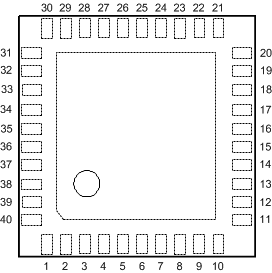
RSB Package
40-Pin WQFN
Top View

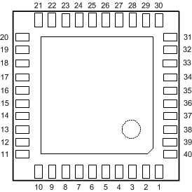
RSB Package
40-Pin WQFN
Bottom View

Pin Functions
| PIN | I/O | TYPE(1) | DESCRIPTION | |
|---|---|---|---|---|
| NUMBER | NAME(2) | |||
| 1 | PWR_ON | I | D | This is an active HI push button input which can be used to signal PWR_ON and PWR_OFF events to the CPU by controlling the EXT_WAKEUP [pin4] and select contents of register 8H'88. |
| 2 | nTEST_JIG | I | D | This is an active LOW input signal used for detecting an external HW event. The response is seen in the EXT_WAKEUP [pin4] and select contents of register 8H'88. |
| 3 | SPARE | I | D | This is an input signal used for detecting a external HW event. The response is seen in the EXT_WAKEUP [pin4] and select contents of register 8H'88. The polarity on this pin is assignable. |
| 4 | EXT_WAKEUP | O | D | This pin generates a single 10-ms pulse output to CPU in response to input from pins 1, 2, and 3. Flags CPU to interrogate register 8H'88. |
| 5 | FB1 | I | A | Buck1 input feedback pin. |
| 6 | VIN | I | PWR | Battery input (internal circuitry and LDO1-3 power input) |
| 7 | VOUT LDO1 | O | PWR | LDO1 output |
| 8 | VOUT LDO2 | O | PWR | LDO2 output |
| 9 | nRSTI | I | D | Active low reset pin. Signal used to reset the device (by default is pulled high internally). Typically a push button reset. |
| 10 | GND1 | G | G | Ground |
| 11 | VREF | O | A | Bypass capacitor for the high internal impedance reference. |
| 12 | VOUT LDO3 | O | PWR | LDO3 output |
| 13 | VOUT LDO4 | O | PWR | LDO4 output |
| 14 | VIN LDO4 | I | PWR | Power input to LDO4 — this can be connected to either from a 1.8-V supply to main battery supply. |
| 15 | VIN BUBATT | I | PWR | Backup battery input supply. |
| 16 | VOUT LDO_RTC | O | PWR | LDO_RTC output supply to the RTC of the application processor. |
| 17 | nBATT_FLT | O | D | Main battery fault output, indicates the main battery is low (discharged) or the DC source has been removed from the system. This gives the processor an indicator that the power will shut down. During this time the processor will operate from the backup coin cell. |
| 18 | PGND2 | G | G | Buck2 NMOS power ground |
| 19 | SW2 | O | PWR | Buck2 switcher output |
| 20 | VIN BUCK2 | I | PWR | Battery input power to Buck2 |
| 21 | SDA | I/O | D | I2C Data (Bidirectional) |
| 22 | SCL | I | D | I2C Clock |
| 23 | FB2 | I | A | Buck2 input feedback pin |
| 24 | nRSTO | O | D | Reset output from the PMIC to the processor |
| 25 | VOUT LDO5 | O | PWR | LDO5 output |
| 26 | VIN LDO5 | I | PWR | Power input to LDO5, this can be connected to VIN or to a separate 1.8-V supply. |
| 27 | VDDA | I | PWR | Analog Power for VREF, BIAS |
| 28 | FB3 | I | A | Buck3 Feedback |
| 29 | GPIO1 / nCHG_EN | I/O | D | General purpose I/O / Ext. backup battery charger enable pin. This pin enables the main battery or DC source power to charge the backup battery. This pin toggled via the application processor. By grounding this pin the DC source continuously charges the backup battery. |
| 30 | GPIO2 | I/O | D | General purpose I/O |
| 31 | VIN BUCK3 | I | PWR | Battery input power to Buck3 |
| 32 | SW3 | O | PWR | Buck3 switcher output |
| 33 | PGND3 | G | G | Buck3 NMOS Power ground |
| 34 | BGND1,2,3 | G | G | Bucks 1, 2 and 3 analog ground |
| 35 | SYNC | I | D | Frequency synchronization: Connection to an external clock signal PLL to synchronize the PMIC internal oscillator. |
| 36 | SYS_EN | I | D | Input digital enable pin for the high voltage power domain supplies. Output from the Monahans processor. |
| 37 | PWR_EN | I | D | Digital enable pin for the low-voltage domain supplies. Output signal from the Monahans processor |
| 38 | PGND1 | G | G | Buck1 NMOS power ground |
| 39 | SW1 | O | PWR | Buck1 switcher output |
| 40 | VIN BUCK1 | I | PWR | Battery input power to Buck1 |
(1) A: Analog Pin D: Digital Pin G: Ground Pin P: Power Pin I: Input Pin I/O: Input/Output Pin O: Output Pin
(2) In this document, active-low logic items are prefixed with a lowercase "n".