SNVS185F February 2002 – April 2017 LP3982
PRODUCTION DATA.
- 1 Features
- 2 Applications
- 3 Description
- 4 Revision History
- 5 Pin Configuration and Functions
- 6 Specifications
- 7 Detailed Description
- 8 Application and Implementation
- 9 Power Supply Recommendations
- 10Layout
- 11Device and Documentation Support
- 12Mechanical, Packaging, and Orderable Information
パッケージ・オプション
メカニカル・データ(パッケージ|ピン)
サーマルパッド・メカニカル・データ
発注情報
6 Specifications
6.1 Absolute Maximum Ratings
over operating free-air temperature range (unless otherwise noted)(1)(2)(3)| MIN | MAX | UNIT | ||
|---|---|---|---|---|
| VIN, VOUT, VSHDN, VSET, VCC, VFAULT | −0.3 | 6.5 | V | |
| Fault sink current | 20 | mA | ||
| Power dissipation | See(4) | |||
| Junction temperature, TJ | 150 | °C | ||
| Storage temperature, Tstg | –65 | 160 | °C | |
(1) Stresses beyond those listed under Absolute Maximum Ratings may cause permanent damage to the device. These are stress ratings only, which do not imply functional operation of the device at these or any other conditions beyond those indicated under Recommended Operating Conditions. Exposure to absolute-maximum-rated conditions for extended periods may affect device reliability.
(2) All voltages are with respect to the potential at the GND pin.
(3) If Military/Aerospace-specified devices are required, contact Texas Instruments Sales Office/Distributors for availability and specifications.
(4) In applications where high power dissipation and/or poor thermal resistance is present, the maximum ambient temperature may have to be derated. Maximum ambient temperature (TA(MAX)) is dependant on the maximum operating junction temperature (TJ(MAX-OP)), the maximum power dissipation (PD(MAX)), and the junction-to-ambient thermal resistance in the application (RθJA). This relationship is given by: TA(MAX) = TJ(MAX-OP) − (PD(MAX) × RθJA).The value of the RθJA for the WSON package is specifically dependent on the PCB trace area, trace material, and the number of layers and thermal vias. For improved thermal resistance and power dissipation for the WSON package, refer to TI Application Note AN-1187 Leadless Leadframe Package (LLP) (SNOA401).
6.2 ESD Ratings
| VALUE | UNIT | |||
|---|---|---|---|---|
| V(ESD) | Electrostatic discharge | Human-body model (HBM), per ANSI/ESDA/JEDEC JS-001(1) | ±2000 | V |
| Machine model | ±200 | V | ||
(1) JEDEC document JEP155 states that 500-V HBM allows safe manufacturing with a standard ESD control process.
6.3 Recommended Operating Conditions(1)(2)
| MIN | NOM | MAX | UNIT | |
|---|---|---|---|---|
| Operating temperature | –40 | 85 | °C | |
| Supply voltage | 2.5 | 6 | V |
6.4 Thermal Information
| THERMAL METRIC(1) | LP3982 | UNIT | ||
|---|---|---|---|---|
| DGK (VSSOP) | NGM (WSON)(2) | |||
| 8 PINS | 8 PINS | |||
| RθJA(3) | Junction-to-ambient thermal resistance, High-K | 175.2 | 52.6 | °C/W |
| RθJC(top) | Junction-to-case (top) thermal resistance | 66.0 | 66.2 | °C/W |
| RθJB | Junction-to-board thermal resistance | 95.6 | 16.7 | °C/W |
| ψJT | Junction-to-top characterization parameter | 9.7 | 1.9 | °C/W |
| ψJB | Junction-to-board characterization parameter | 94.2 | 16.7 | °C/W |
| RθJC(bot) | Junction-to-case (bottom) thermal resistance | n/a | 11.1 | °C/W |
(1) For more information about traditional and new thermal metrics, see the Semiconductor and IC Package Thermal Metrics application report.
(2) The PCB for the WSON/NGN package RθJA includes thermal vias under the exposed thermal pad per EIA/JEDEC JESD51-5.
(3) Thermal resistance value RθJA is based on the EIA/JEDEC High-K printed circuit board defined by: JESD51-7 - High Effective Thermal Conductivity Test Board for Leaded Surface Mount Packages.
6.5 Electrical Characteristics
Unless otherwise specified, all limits are specified for VIN = VOUT + 0.5 V(1), VSHDN = VIN, CIN = COUT = 2.2 μF, CCC = 33 nF, TJ = 25°C.| PARAMETER | TEST CONDITIONS | MIN(2) | TYP(3) | MAX(2) | UNIT | |
|---|---|---|---|---|---|---|
| VIN | Input voltage | For operating temperature extremes: −40°C to 85°C | 2.5 | 6 | V | |
| ΔVOUT | Output voltage tolerance | 100 μA ≤ IOUT ≤ 300 mA VIN = VOUT + 0.5 V(1) SET = OUT for the ADJ Versions |
−2 | 2 | % of VOUT (NOM) | |
| For operating temperature extremes: −40°C to 85°C | −3 | 3 | ||||
| VOUT | Output adjust range | ADJ version only; for operating temperature extremes: −40°C to 85°C |
1.25 | 6 | V | |
| IOUT | Maximum output current | Average DC current rating; For operating temperature extremes: −40°C and 85°C |
300 | mA | ||
| ILIMIT | Output current limit | 770 | mA | |||
| For operating temperature extremes: −40°C to 85°C | 330 | |||||
| IQ | Supply current | IOUT = 0 mA | 90 | μA | ||
| IOUT = 0 mA; for operating temperature extremes: −40°C to 85°C |
270 | |||||
| IOUT = 300 mA | 225 | |||||
| Shutdown supply current | VO = 0 V, SHDN = GND | 0.001 | 1 | μA | ||
| VDO | Dropout voltage(1)(4) | IOUT = 1 mA | 0.4 | mV | ||
| IOUT = 200 mA | 80 | |||||
| IOUT = 200 mA; for operating temperature extremes: −40°C to 85°C |
220 | |||||
| IOUT = 300 mA | 120 | |||||
| ΔVOUT | Line regulation | IOUT = 1 mA, (VOUT + 0.5 V) ≤ VI ≤ 6 V(1) |
0.01 | %/V | ||
| IOUT = 1 mA, (VOUT + 0.5 V) ≤ VI ≤ 6 V(1); for operating temperature extremes: −40°C to 85°C |
−0.1 | 0.1 | ||||
| Load regulation | 100 μA ≤ IOUT ≤ 300 mA | 0.002 | %/mA | |||
| en | Output voltage noise | IOUT = 10 mA, 10 Hz ≤ f ≤ 100 kHz | 37 | μVRMS | ||
| Output voltage noise density | 10 Hz ≤ f ≤ 100 kHz, COUT = 10 μF | 190 | nV/√Hz | |||
| VSHDN | SHDN input threshold | VIH, (VOUT + 0.5 V) ≤ VIN ≤ 6 V(1); for operating temperature extremes: −40°C to 85°C |
2 | V | ||
| VIL, (VOUT + 0.5 V) ≤ VIN ≤ 6 V(1); for operating temperature extremes:−40°C to 85°C |
0.4 | |||||
| ISHDN | SHDN input bias current | SHDN = GND or IN | 0.1 | 100 | nA | |
| ISET | SET input leakage | SET = 1.3 V, ADJ version only(5) | 0.1 | 2.5 | nA | |
| VFAULT | FAULT detection voltage | VO ≥ 2.5 V, IOUT = 200 mA(6) | 120 | mV | ||
| VOUT ≥ 2.5 V, IOUT = 200 mA(6); for operating temperature extremes: −40°C to 85°C |
280 | |||||
| FAULT output low voltage | ISINK = 2 mA | 0.115 | V | |||
| ISINK = 2 mA; for operating temperature extremes: −40°C to 85°C |
0.25 | |||||
| IFAULT | FAULT off-leakage current | FAULT = 3.6 V, SHDN = 0 V | 0.1 | 100 | nA | |
| TSD | Thermal shutdown temperature | 160 | °C | |||
| Thermal shutdown hysteresis | 10 | |||||
| TON | Start-up time | COUT = 10 μF, VOUT at 90% of final value | 120 | μs | ||
(1) Condition does not apply to input voltages below 2.5 V because this is the minimum input operating voltage.
(2) All limits are verified by testing or statistical analysis.
(3) Typical values represent the most likely parametric norm.
(4) Dropout voltage is measured by reducing VIN until VOUT drops 100 mV from its nominal value at VIN – VOUT = 0.5 V. Dropout voltage does not apply to the 1.8-V version.
(5) The SET pin is not externally connected for the fixed versions.
(6) The FAULT detection voltage is specified for the input-to-output voltage differential at which the FAULT pin goes active low.
6.6 Typical Characteristics
Unless otherwise specified, VIN = VO + 0.5 V, CIN = COUT = 2.2 μF, CCC = 33 nF, TJ = 25°C, VSHDN = VIN.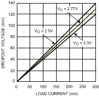 Figure 1. Dropout Voltage vs Load Current
(for Different Output Voltages)
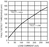 Figure 3. FAULT Detect Threshold vs Load Current
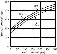 Figure 5. Supply Current vs Load Current
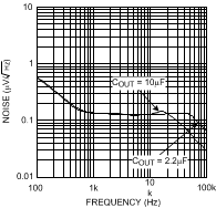 Figure 7. Output Noise Spectral Density
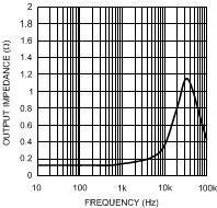 Figure 9. Output Impedance vs Frequency
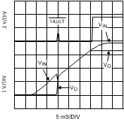 Figure 11. Power-Up Response
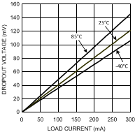 Figure 2. Dropout Voltage vs Load Current
(for Different Output Temperatures)
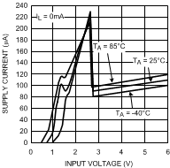 Figure 4. Supply Current vs Input Voltage
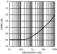 Figure 6. Power Supply Rejection Ratio vs Frequency
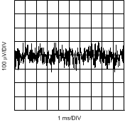 Figure 8. Output Noise (10 Hz to 100 kHz)
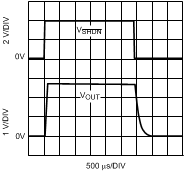 Figure 10. Shutdown Response
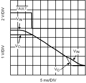 Figure 12. Power-Down Response