SNVS440B May 2007 – March 2016 LP5520
PRODUCTION DATA.
- 1 Features
- 2 Applications
- 3 Description
- 4 Revision History
- 5 Pin Configuration and Function
-
6 Specifications
- 6.1 Absolute Maximum Ratings
- 6.2 ESD Ratings
- 6.3 Recommended Operating Conditions
- 6.4 Thermal Information
- 6.5 Electrical Characteristics
- 6.6 RGB Driver Electrical Characteristics (ROUT, GOUT, BOUT Outputs)
- 6.7 Logic Interface Characteristics
- 6.8 Magnetic Boost DC-DC Converter Electrical Characteristics
- 6.9 I2C Timing Parameters
- 6.10 SPI Timing Requirements
- 6.11 Typical Characteristics
- 7 Detailed Description
- 8 Application and Implementation
- 9 Power Supply Recommendations
- 10Layout
- 11Device and Documentation Support
- 12Mechanical, Packaging, and Orderable Information
7 Detailed Description
7.1 Overview
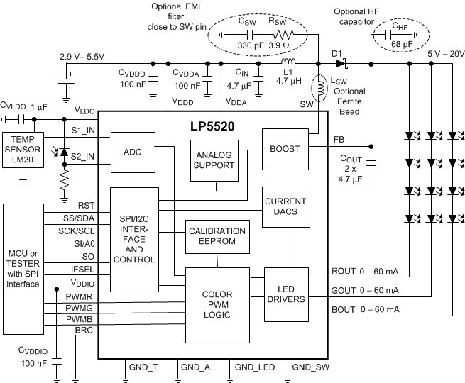
The LP5520 is an RGB backlight LED driver for small format color LCDs. The LP5520 offers a small and simple driver solution without need for optical feedback. Calibration in display module production can be done in one temperature. The LP5520 produces true white light over a wide temperature range.
Three independent LED drivers have accurate programmable current sinks with up to 60 mA current capability and PWM modulation control. Using internal calibration memory and external temperature sensor, the RGB LED currents are adjusted for perfect white balance independent of the brightness setting or temperature. The user programmable calibration memory has intensity vs temperature data for each color. This white balance calibration data can be programmed to the memory on the production line of a backlight module.
The LP5520 has a magnetic boost converter that creates supply voltage up to 20-V LED from the battery voltage. The output can be set at 1-V step from 5 V to 20 V. In adaptive mode the circuit automatically adjusts the output voltage to minimum sufficient level for lowest power consumption.
Temperature is measured using an external temperature sensor placed close to the LEDs. The second ADC input can be used, for example, for ambient light measurement.
7.2 Functional Block Diagram
7.3 Feature Description
7.3.1 Start-Up Powering
VDDD and VDDA must be tied together and turned on first. VDDIO must be turned on at the same time as VDDD or later. In the power-off sequence VDDIO must be turned off before VDDD or at the same time.
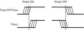 Figure 9. Power-On Signal Timing
7.3.2 RGB Driver Functionality
7.3.2.1 White Balance Control
The LP5520 is designed to provide spectrally rich white light using a three-color RGB LED. White light is obtained when the red, green, and blue LED intensities are in proper balance. The LED intensities change independently with temperature. For maintaining the purity of the white color and the targeted total intensity, precise temperature dependent intensity control for each LED is required. The color coordinates in this document refer to the CIE 1931 color graph (x,y system).
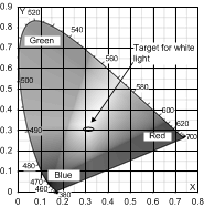 Figure 10. CIE 1931 Color Graph
Figure 11 shows a typical RGB LED intensity behavior on a 12-bit scale (0 to 4095) at constant 20-mA LED currents. Figure 12 shows the typical color coordinate change for an uncompensated RGB LED. Figure 13 shows the corresponding PWM values for achieving constant intensity white light across the temperature range. The PWM values have been saturated at 104°C to avoid overheating the LED and to better utilize the PWM range. The white balance is not maintained above 104°C in this case.
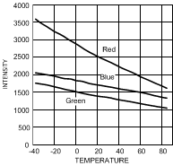 Figure 11. LED Intensity vs Temperature
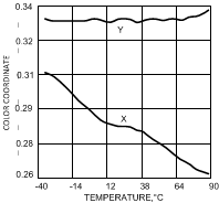 Figure 12. Typical Color Coordinates vs Temperature for Uncompensated RGB LED
The compensation values for the measured temperatures can be easily calculated when the intensity vs temperature information is available. For the best accuracy the iterative calibration approach must be used.
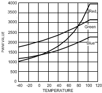 Figure 13. Compensation PWM Values
The compensation values must be converted to 16°C intervals when they are programmed to the calibration EEPROM. The evaluation software has import function, which can be used to convert the measured compensation data to the 16°C interval format. The measured data can have any temperature points, and the software fits a curve through the measured points and calculate new PWM values in fixed temperatures using the curves.
Typical color coordinate and intensity stability over temperature are shown in Figure 14 and Figure 15.
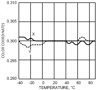 Figure 14. Compensated Color Coordinates vs Temperature
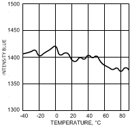 Figure 15. Compensated Blue LED Intensity vs Temperature
7.3.2.2 LED Brightness Control
The LED brightness is defined by two factors, the current through the LED and the PWM duty cycle. The constant current outputs ROUT, GOUT, and BOUT can be independently set to sink between 0 and 60 mA. The 8-bit current control has 255 levels, and the step size is 235 µA. In manual mode the current is defined with the current control (R/G/B) registers (01H, 02H, and 03H). In automatic mode the current settings are loaded from the EEPROM.
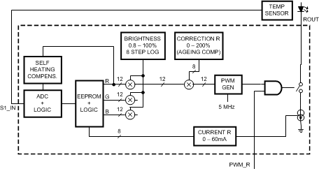
The PWM control has 12-bit resolution, which means 4095 steps. The minimum pulse width is 200 ns, and the frequency can be set to either 1.2 kHz or 19.2 kHz. The duty cycle range is from 0 to 100% (0 to 4095). The output PWM value is obtained by multiplication of three factors. The first factor is the temperature-based value from the EEPROM. The second factor is the correction register setting, which is independent for each color. The third factor is the brightness register setting, which is common to all colors.
The temperature-based PWM values are stored in the EEPROM at 16°C intervals starting from –40°C and ending to 120°C. PWM values for the temperatures between the stored points are interpolated.
LED brightness has 3-bit logarithmic control. The control bits are in the pwm_brightness (04H) register. The 3-bit value defines a multiplier for the 12-bit PWM value obtained from the memory according to Table 1.
Table 1. PWM Value Multipliers
| CONTROL BYTE <bri[2:0]>(1) | MULTIPLIER | INTENSITY ( %) |
|---|---|---|
| 0 | 0.008 | 0.8 |
| 1 | 0.016 | 1.6 |
| 2 | 0.031 | 3.1 |
| 3 | 0.063 | 6.3 |
| 4 | 0.125 | 12.5 |
| 5 | 0.250 | 25 |
| 6 | 0.500 | 50 |
| 7 | 1.000 | 100 |
The brightness correction can be used for aging compensation or other fine-tuning. There is an 8-bit correction register for each output. The PWM value obtained from the memory is multiplied by the correction value. The default correction value is 1. Correction range is from 0 to 2 and the LSB is 0.78% (1/128).
7.3.2.3 LED PWM Control
The PWM frequency can be selected of two alternatives, slow and fast, with the control bit <pwm_fast>. The slow frequency is 1.2 kHz. In the fast mode the PWM frequency is multiplied by 16, and the frequency is 19.2 kHz. Fast mode is the default mode after reset. The single pulse in normal PWM is split in 16 narrow pulses in fast PWM. Higher frequency helps eliminate possible noise from the ceramic capacitors and it also reduces the ripple in the boost voltage. Minimum pulse length is 200 ns in both modes.
The PWM pulses of each output do not start simultaneously in order to avoid high current spike. Red starts in the beginning of the PWM cycle, Green is symmetric with the cycle center and Blue ends in the end of the cycle. For PWM values less than 33% for each output, the output currents are completely non-overlapping. With higher PWM values the overlapping increases.
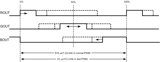 Figure 17. Pulse Positions in the PWM Cycle
7.3.2.4 Sequential Mode
Completely non-overlapping timing can be obtained by using the sequential mode as shown in Figure 18. The timing is defined with external PWM control inputs. The minimum trigger pulse width in the PWM inputs is 1 µs. There is no limitation on the maximum width of the pulse as long as it is shorter than the whole sequence.
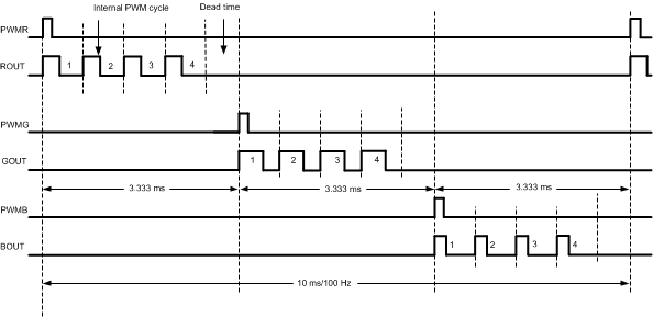 Figure 18. Non-Overlapping External Synchronized Sequential Mode
In sequential mode the PWM cycle is synchronized to trigger pulses and the amount of PWM pulses per trigger can be defined to 2, 3 or 4 using the <seq_mode0> and <seq_mode1> control bits. This makes possible to use sequence lengths of about 5 ms, 7.5 ms or 10 ms. Fast PWM can be used in sequential mode, but the frame timing is as with normal PWM.
The PWM timing and synchronization timing originate from different clock sources. Some margin must be allowed for clock tolerances. This margin shows as a dead time in the waveform graph. Some dead time must be allowed so that no PWM pulse is clipped. Clipping would distort the intensity balance between the LEDs. The dead time causes some intensity reduction, but assures the current balance.
PWM mode is defined by <seq_mode1> and <seq_mode2> control bits of rgb_control (00H) register:
Table 2. PWM Mode
| <seq_mode1> (BIT 7) |
<seq_mode0> (BIT 6) |
MODE |
|---|---|---|
| 0 | 0 | Normal mode |
| 0 | 1 | Sequential mode with 2 PWM pulses per trigger |
| 1 | 0 | Sequential mode with 3 PWM pulses per trigger |
| 1 | 1 | Sequential mode with 4 PWM pulses per trigger |
7.3.2.5 Current Control of the LEDs
The LP5520 has a separate 8-bit current control for each LED output. In manual mode the current for red LED is controlled with the current_control_r (01H) register, the green LED is controlled with the current_control_g (02H), and the blue LED with current_control_b (03H). Output current can be calculated with formula: current (mA) = code × 0.235; for example, a 20-mA current is obtained with code 85 (55H).
In automatic and stand-alone modes the LED current values programmed in EEPROM are used, and the current control registers have no effect. There are two ways to change the default current if needed. The defaults can be changed permanently by programming new values to the EEPROM. The other option is to make a temporary change by writing new current values in SRAM.
7.3.2.6 Output Enables
ROUT, GOUT, and BOUT output activity is controlled with 3 enable bits of the rgb_control (00H) register:
Table 3. Output Enable Bits
| <en_b> (bit 2) | 0 | Blue LED output BOUT disabled |
| 1 | Blue LED output BOUT enabled | |
| <en_g> (bit 1) | 0 | Green LED output GOUT disabled |
| 1 | Green LED output GOUT enabled | |
| <en_r> (bit 0) | 0 | Red LED output ROUT disabled |
| 1 | Red LED output ROUT enabled |
PWM control inputs PWMR, PWMG and PWMB can be used as external output enables in normal and automatic mode. In the sequential mode these inputs are the trigger inputs for respective outputs.
7.3.2.7 Fade In and Fade Out
The LP5520 has an automatic fade in and out for the LED outputs. Fading makes the transitions smooth in on and off switching or when brightness is changed. It is not applied for the changes caused by the compensation algorithm. The fade can be turned on and off using the <en_fade> bit in the rgb_control (00H) register. The fade time is constant 520 ms, and it does not depend on how big the brightness change is. The white balance is maintained during fading. Fading is off in the stand-alone mode.
Table 4. Fade In and Fade Out With <en_fade> Bit
| <en_fade>(bit 5) | 0 | Automatic fade disabled |
| 1 | Automatic fade enabled |
Fading only works in automatic mode. The LED current registers must be written to 0 for proper fade operation. When the LEDs are turned on with fading, it is best to set the brightness first and then enable the outputs and automatic mode. The LEDs can be turned off then by turning off the automatic mode (write rgb_auto to 0).
7.3.2.8 Temperature and Light Measurement
The LP5520 has a 12-bit analog-to-digital converter (ADC) for the measurements. The ADC has two inputs. S1_IN input is intended for the LM20 temperature sensor and S2_IN input for light measurement or any DC voltage measurement. The conversion results are filtered with average filter for 134 ms. The <adc_ch> bit in the Control register selects, which conversion result can be read out from the registers ADC_hi_byte and ADC_low_byte. The ADC_hi_byte must be read first. The <comp_ch> bit selects, which input is used for compensation. The ADC uses the LDO voltage 2.8 V as the reference voltage. The input signal range is 0 V to 2.8 V, and the inputs are buffered on the chip.
If S2_IN is used for light measurement using TDK optical sensor BCS2015G1 as shown in the Functional Block Diagram, the measurement range is from 10 to 20 000 lux when using a 100-kΩ resistor.
Table 5. ADC Configuration
| adc_ch(bit5) | 0 | S1 input can be read |
| 1 | S2 input can be read | |
| comp_sel(bit4) | 0 | S1 input is used for compensation |
| 1 | S2 input is used for compensation |
 Figure 19. ADC Operation Block Diagram
7.3.3 Magnetic High-Voltage Boost DC-DC Converter
The LP5520 boost DC-DC converter generates a 5-V to 20-V supply voltage for the LEDs from single Li-Ion battery (2.9 V to 4.5V). The output voltage is controlled with four bits in 18 steps. In adaptive mode the output voltage is automatically adjusted so that the LED drivers have enough voltage for proper operation. The converter is a magnetic switching PWM mode DC-DC converter with a current limit. Switching frequency is 1 MHz. Boost converter options are controlled with few bits of Control (06H) register.
Table 6. Boost DC-DC Converter Control
| <en_autoload> (bit 3) | 0 | Internal boost converter loader off |
| 1 | Internal boost converter loader on | |
| <vout_auto> (bit 2) | 0 | Manual boost output adjustment |
| 1 | Adaptive boost output adjustment | |
| <en_boost> (bit 1) | 0 | Boost converter standby mode |
| 1 | Boost converter active mode | |
| <nstby> (bit 0) | 0 | LP5520 standby mode |
| 1 | LP5520 active mode |
The LP5520 boost converter uses pulse-skipping elimination to stabilize the noise spectrum. Even with light load or no load a minimum length current pulse is fed to the inductor. An active load is used to remove the excess charge from the output capacitor at very light loads. Active load can be disabled with the <en_autoload> bit. Disabling active load increases slightly the efficiency at light loads, but the downside is that pulse skipping occurs. The boost converter must be stopped when there is no load to minimize the current consumption.
The topology of the magnetic boost converter is called current programmed mode (CPM) control, where the inductor current is measured and controlled with the feedback. The user can program the output voltage of the boost converter. The output voltage control changes the resistor divider in the feedback loop.
Figure 20 shows the boost topology with the protection circuitry. Four different protection schemes are implemented:
- Overvoltage protection: limits the maximum output voltage and:
- Keeps the output below breakdown voltage.
- Prevents boost operation if battery voltage is much higher than desired output.
- Overcurrent protection: limits the maximum inductor current and:
- Voltage over switching NMOS is monitored; voltages too high turn off the switch.
- Feedback break protection: prevents uncontrolled operation if FB pin is disconnected.
- Duty cycle limiting done with digital control.
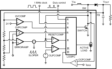 Figure 20. Boost Converter Topology
7.3.3.1 Boost Control
User can set the boost converter to standby mode by writing the register bit <en_boost> low. When <en_boost> is written high, the converter starts for 50 ms in low current PWM mode and then goes to normal PWM mode.
User can control the boost output voltage by boost output boost_output (05H) register.
Table 7. Boost Output Voltage Control
| BOOST OUTPUT [7:0] REGISTER 0DH |
BOOST OUTPUT VOLTAGE (TYPICAL) |
|
| Bin | Dec | |
| 00101 | 5 | 5 V |
| 00110 | 6 | 6 V |
| 00111 | 7 | 7 V |
| ... | ... | ... |
| 01100 | 12 | 12 V |
| 01101 | 13 | 13 V |
| 01110 | 14 | 14 V |
| ... | ... | ... |
| 10010 | 18 | 18 V |
| 10011 | 19 | 19 V |
| 10100 | 20 | 20 V |
If register value is lower than 5, then value of 5 is used internally. If register value is higher than 20, then value of 20 is used internally.
7.3.3.2 Adaptive Output Voltage Control
When automatic boost voltage control is selected using the <vout_auto> bit in the Control (06H) register, the user-defined boost output voltage is ignored. The boost output voltage is adjusted for sufficient operating headroom by monitoring all enabled LED driver outputs. The boosted voltage is adjusted so that the lowest driver voltage is from 0.85 V to 1.35 V when the LED output currents are below 30 mA and from 1 V to 1.5V when any LED current is above 30 mA. The output voltage range is from 5 V to 20 V in adaptive mode.
The adaptive voltage control helps saving energy by always setting the boost voltage to minimum sufficient value. It eliminates the need for extra voltage margins due to LED forward voltage variation or temperature variation. With very small brightness settings, when the PWM pulses in LED outputs are very narrow, the adaptive voltage setting gives higher than necessary boost voltage. This does not harm the overall efficiency, because this happens only at low power levels.
After reset the adaptive control is on by default. In stand-alone mode the adaptive output voltage is always used.
7.4 Device Functional Modes
The LP5520 has three different operating modes: manual mode, automatic mode, and stand-alone mode. Automatic mode has two sub modes: normal mode and sequential mode. In manual and automatic modes the device is controlled through the serial interface. In stand-alone mode only BRC input must be controlled, and all registers have the default values. The modes are controlled according Table 8.
Table 8. Device Operating Modes Control
| <RGB_auto> (RBG control bit 3) |
<seq_mode[0:1]> (RBG control bits 6 and 7) |
DEVICE OPERATING MODE |
| 0 | 00 | Manual mode |
| 1 | 00 | Automatic mode, normal operation (overlapping) |
| 1 | 01, 10, or 11 | Automatic mode, sequential operation with 2, 3, or 4 pulses per sequence |
7.4.1 Manual Mode
In the manual mode the automatic LED intensity adjustment is not in use. The internal PWM control is disabled, and the LEDs are driven with DC current. The user can set the LED currents through the serial port using three current control registers, current_control_R/G/B, and use the external PWM control inputs to adjust LED intensities if needed. There is an independent PWM control pin for each output. If PWM control is not used, the PWMR, PWMG, and PWMR inputs must be tied to the VDDIO. All the functions implemented with the internal PWM control are unavailable in manual mode (logarithmic brightness control from PWM Control register, temperature compensation, fading, sequential mode).
7.4.2 Automatic Mode
In the automatic mode the LED intensities are controlled with the 12-bit PWM values obtained from the EEPROM memory according to the temperature information. PWM values are stored at 16°C intervals for the
–40°C to +120°C temperature range, and the PWM values for the intermediate temperatures are linearly interpolated.
When creating white light from a RGB LED, the intention is to program PWM values, which keep the individual LED intensities constant in all temperatures. For possible other applications, other kind of PWM behavior can be programmed. The variable parameter can be other than temperature if the sensor is changed to, for example, a light sensor.
12-bit ADC is used for the measurements. The ADC has two inputs: S1_IN and S2_IN. The temperature measurement result from the S1_IN input is converted to EEPROM address using the sensor calibration data from EEPROM. This EEPROM address is then used to get the PWM values for each output. The second input S2_IN can be used for example for ambient light measurement. The ADC data from selected input can be read through the serial interface. Control bit <comp_sel> can be used to select which input is used for compensation.
Current setting for each LED comes from EEPROM in the automatic mode. The same current values must be programmed as were used in the calibration. Current control range is from 0 to 60 mA with 8-bit resolution and the step size is 235 µA.
Common brightness control for all LEDs can be done using the pwm_brightness (05H) register. The pwm_brightness register makes 8 level logarithmic brightness control with 3 bits. An automatic fade function allows smooth turnon, turnoff, and brightness changes of the LEDs. White balance is maintained during fading.
A brightness correction value can be given for each LED. The PWM value obtained from the EEPROM memory is multiplied by this correction value. This feature can be used for example for LED aging compensation or for color adjustment by user. These values are kept in R_correction (0AH), G_correction (0BH) and B_correction (0CH) registers. The correction multiplier can be between 0 and 2.
Due to LED self-heating, the temperature sensor and the LED temperatures will differ. The difference depends on the thermal structure of the display module and the distance between the sensor and the LEDs. This temperature difference can be compensated by storing the temperature difference value at highest power (100% red LED PWM) in the EEPROM memory. The system then corrects the measured temperature based on the actual PWM value used. The correction assumes that the red LED PWM value is representing the whole RGB LED power consumption.
Sequential (non-overlapping) drive is possible using external PWM control inputs to trigger a new sequence in each LED output. 60 mA maximum current setting makes possible 20 mA maximum averaged current for each output in the non-overlapping mode.
7.4.3 Stand-Alone Mode
In stand-alone mode the operation is controlled through a single PWM brightness input, BRC. After power-up or reset the LP5520 is ready for stand-alone operation without any setup through the serial interface. The stand-alone mode is entered with a rising edge in the BRC input. The boost converter operates in adaptive mode. The LED current settings are loaded from EEPROM. The LED brightness is controlled with a PWM signal in the BRC input. The BRC PWM frequency must be from 2 to 10 kHz. The PWM signal in the BRC input is not used as such for the LED outputs, but it is converted to 3-bit value and a logarithmic brightness control is based on this 3-bit value, as shown in Table 9. There is hysteresis in the conversion to avoid blinking when the BRC duty cycle is close to a threshold. When the PWM pulses end in the BRC input and the input stays low, the circuit goes to the standby mode.
Figure 21 shows the waveforms in BRC input and ROUT output in the stand-alone mode. The circuit is in standby mode until the first rising edge in BRC input is detected. The circuit starts up, and the outputs activate after 30 ms from the first rising edge in BRC. The BRC frequency is assumed to 2 kHz in this example giving 0.5 ms BRC period. When the duty cycle changes in BRC, it takes two BRC periods before the change is reflected in the output. When BRC goes permanently low, the circuit enters standby mode after 15 ms from the last BRC pulse.
All controls through the serial interface can be used in the stand-alone mode. In Automatic and Manual mode the control bit <brc_off> must be written high and BRC input kept low to prevent the LP5520 device from entering stand-alone mode.
Table 9. Stand-Alone Mode Brightness Control
| BRC DUTY CYCLE THRESHOLD VALUES (%) | INTENSITY (% of maximum) |
RECOMMENDED BRC PWM CONTROL VALUES | ||
|---|---|---|---|---|
| INCREASING | DECREASING | INCREASING | DECREASING | |
| 0 | off | 0 | ||
| 1 | 15 | 0.8 | 10 | 10 |
| 20 | 28 | 1.6 | 28 | 22 |
| 35 | 42 | 3.1 | 40 | 32 |
| 48 | 52 | 6.3 | 53 | 47 |
| 58 | 62 | 12.5 | 63 | 58 |
| 68 | 75 | 25 | 75 | 70 |
| 82 | 90 | 50 | 88 | 85 |
| 97 | 100 | 99 | ||
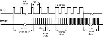 Figure 21. LP5520 Control and Output Waveforms in Stand-Alone Mode
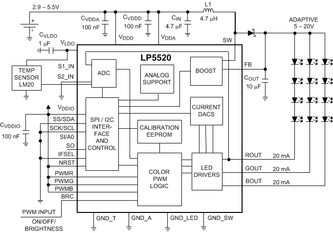 Figure 22. LP5520 Connections in Stand-Alone Mode
7.4.4 Start-Up Sequence
-
RESET: In the RESET mode all the internal registers are reset to the default values, and the chip goes to STANDBY mode after reset. <NSTBY> control bit is low after reset by default. Reset is entered always if NRST input is low or internal power on reset (POR) is active. POR activates during the chip start-up or when the supply voltage VDD falls below 1.5 V. Once VDD rises above 1.5 V, POR inactivates, and the device continues to the STANDBY mode.
-
STANDBY: The STANDBY mode is entered if the register bit <NSTBY> is LOW. This is the low-power consumption mode, when all circuit functions are disabled. Registers can be written in this mode, and the control bits are effective immediately after power up.
-
STARTUP: When <NSTBY> bit is written high or there is a rising edge in the BRC input, the INTERNAL STARTUP SEQUENCE powers up all the needed internal blocks (Vref, Bias, Oscillator, etc.). To ensure the correct initialization, a 10-ms delay is generated by the internal state-machine after the trim EEPROM values are read. If the chip temperature rises too high, the thermal shutdown (TSD) disables the chip operation, and STARTUP mode is entered until no TSD event is present.
-
BOOST STARTUP: Soft start for boost output is generated in the BOOST STARTUP mode. The boost output is raised in PWM mode during the 20-ms delay generated by the state machine. All LED outputs are off during the 20-ms delay to ensure smooth start-up. The boost start-up is entered from internal start-up sequence if <EN_BOOST> is HIGH or from Normal mode when <EN_BOOST> is written HIGH.
-
NORMAL: During NORMAL mode the user controls the chip using the control registers or the BRC input in stand-alone mode. The registers can be written in any sequence and any number of bits can be altered in a register in one write.
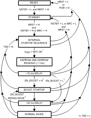 Figure 23. Device Functional Modes
7.5 Programming
7.5.1 Control Interface
The LP5520 supports two different interface modes:
- SPI interface (4-wire, serial), and
- I2C-compatible interface (2-wire, serial)
User can define the serial interface by IF_SEL pin. IF_SEL = 0 selects the I2C mode.
7.5.1.1 I2C Compatible Interface
7.5.1.1.1 I2C Signals
The serial interface is in I2C mode when IF_SEL = 0. The SCL pin is used for the I2C clock and the SDA pin is used for bidirectional data transfer. Both these signals need a pullup resistor according to I2C specification. The values of the pullup resistors are determined by the capacitance of the bus (typical resistance is 1.8 kΩ). Signal timing specifications are shown in I2C Timing Parameters.
7.5.1.1.2 I2C Data Validity
The data on SDA line must be stable during the HIGH period of the clock signal (SCL). In other words, state of the data line can only be changed when CLK is LOW.
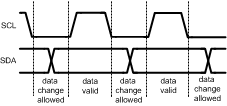 Figure 24. I2C Signals: Data Validity
7.5.1.1.3 I2C Start and Stop Conditions
START and STOP bits classify the beginning and the end of the I2C session. START condition is defined as SDA signal transitioning from HIGH to LOW while SCL line is HIGH. STOP condition is defined as the SDA transitioning from LOW to HIGH while SCL is HIGH. The I2C master always generates START and STOP bits. The I2C bus is considered to be busy after START condition and free after STOP condition. During data transmission, I2C master can generate repeated START conditions. First START and repeated START conditions are equivalent, function-wise.
 Figure 25. I2C Start and Stop Conditions
7.5.1.1.4 Transferring Data
Every byte put on the SDA line must be eight bits long, with the most significant bit (MSB) being transferred first. Each byte of data has to be followed by an acknowledge bit. The acknowledge related clock pulse is generated by the master. The transmitter releases the SDA line (HIGH) during the acknowledge clock pulse. The receiver must pull down the SDA line during the 9th clock pulse, signifying an acknowledge. A receiver which has been addressed must generate an acknowledge after each byte has been received.
After the START condition, the I2C master sends a chip address. This address is seven bits long followed by an eighth bit which is a data direction bit (R/W). The LP5520 address is 20h when SI=0 and 21h when SI=1. For the eighth bit, a 0 indicates a WRITE and a 1 indicates a READ. The second byte selects the register to which the data is written. The third byte contains data to write to the selected register.
 Figure 26. I2C Chip Address
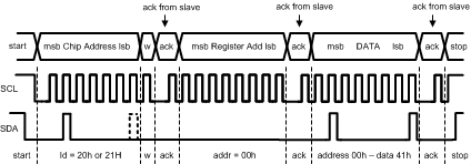
r = read (SDA = 1)
ack = acknowledge (SDA pulled down by either master or slave)
rs = repeated start
id = 7-bit chip address, 20h when SI=0 and 21h when SI=1 for LP5520.
When a READ function is to be accomplished, a WRITE function must precede the READ function, as shown in the I2C Read Cycle waveform.
 Figure 28. I2C Read Cycle
7.5.1.2 SPI Interface
The LP5520 is compatible with SPI serial-bus specification, and it operates as a slave. The transmission consists of 16-bit write and read cycles. One cycle consists of 7 address bits, 1 read/write (RW) bit, and 8 data bits. RW-bit high state defines a write cycle and low defines a read cycle. SO output is normally in high-impedance state, and it is active only when data is sent out during a read cycle. The address and data are transmitted MSB first. The slave select signal (SS) must be low during the cycle transmission. SS resets the interface when high, and it must be taken high between successive cycles. Data is clocked in on the rising edge of the SCK clock signal, while data is clocked out on the falling edge of SCK.
 Figure 29. SPI Write Cycle
 Figure 30. SPI Read Cycle
7.5.1.2.1 SPI Incremental Addressing
The LP5520 supports incremental addressing for memory read and write.
7.5.2 EEPROM Memory
The 1-kbit calibration EEPROM memory is organized as 128 × 8 bits. It stores the 12-bit calibration PWM values for each output at 16°C intervals. Ten temperature points are used to cover the range from –40 to +120°C. The temperature or light sensor calibration data, self-heating factor, and LED currents are also stored in the memory. The memory contents and detailed memory map are shown in Table 10 and Table 11.
Table 10. EEPROM Contents
| DATA | LENGTH | TOTAL BITS |
|---|---|---|
| 10 PWM values for red | 12 | 120 |
| 10 coefficients for red between the points | 8 | 80 |
| 10 PWM values for green | 12 | 120 |
| 10 coefficients for green between the points | 8 | 80 |
| 10 PWM values for blue | 12 | 120 |
| 10 coefficients for blue between the points | 8 | 80 |
| 0°C reading for temperature sensor | 12 | 12 |
| Coefficient for temperature sensor | 12 | 12 |
| Maximum self-heating (100% red PWM) | 8 | 8 |
| Default current for ROUT | 8 | 8 |
| Default current for GOUT | 8 | 8 |
| Default current for BOUT | 8 | 8 |
| Free memory for user data | 8 | 368 |
Table 11. EEPROM Memory Map
| ADDRESS | BITS [7:4] | BITS [3:0] | DEFINITION | |
|---|---|---|---|---|
| 00 | RB0[7:0] | Base PWM value for red (8 LSB bits) |
–40...–25 | |
| 01 | RB1[7:0] | –24...–9 | ||
| 02 | RB2[7:0] | –8...+7 | ||
| 03 | RB3[7:0] | 8...23 | ||
| 04 | RB4[7:0] | 24..39 | ||
| 05 | RB5[7:0] | 40...55 | ||
| 06 | RB6[7:0] | 56...71 | ||
| 07 | RB7[7:0] | 72...87 | ||
| 08 | RB8[7:0] | 88...103 | ||
| 09 | RB9[7:0] | from 104 | ||
| 0a | GB0[7:0] | Base PWM value for green (8 LSB bits) |
–40...–25 | |
| 0b | GB1[7:0] | –24...–9 | ||
| 0c | GB2[7:0] | –8...+7 | ||
| 0d | GB3[7:0] | 8...23 | ||
| 0e | GB4[7:0] | 24..39 | ||
| 0f | GB5[7:0] | 40...55 | ||
| 10 | GB6[7:0] | 56...71 | ||
| 11 | GB7[7:0] | 72...87 | ||
| 12 | GB8[7:0] | 88...103 | ||
| 13 | GB9[7:0] | from 104 | ||
| 14 | BB0[7:0] | Base PWM value for blue (8 LSB bits) |
–40...–25 | |
| 15 | BB1[7:0] | –24...–9 | ||
| 16 | BB2[7:0] | –8...+7 | ||
| 17 | BB3[7:0] | 8...23 | ||
| 18 | BB4[7:0] | 24..39 | ||
| 19 | BB5[7:0] | 40...55 | ||
| 1a | BB6[7:0] | 56...71 | ||
| 1b | BB7[7:0] | 72...87 | ||
| 1c | BB8[7:0] | 88...103 | ||
| 1d | BB9[7:0] | from 104 | ||
| 1e | LM20K[7:0] | Scaling values for LM20 sensor | K | |
| 1f | LM20B[7:0] | B | ||
| 20 | Not used | |||
| ... | ||||
| 3f | ||||
| 40 | RC0[7:0] | Coefficient PWM value for red | –40...–25 | |
| 41 | RC1[7:0] | –24...–9 | ||
| 42 | RC2[7:0] | –8...+7 | ||
| 43 | RC3[7:0] | 8...23 | ||
| 44 | RC4[7:0] | 24..39 | ||
| 45 | RC5[7:0] | 40...55 | ||
| 46 | RC6[7:0] | 56...71 | ||
| 47 | RC7[7:0] | 72...87 | ||
| 48 | RC8[7:0] | 88...103 | ||
| 49 | RC9[7:0] | From 104 | ||
| 4a | GC0[7:0] | Coefficient PWM value for green | –40...–25 | |
| 4b | GC1[7:0] | –24...–9 | ||
| 4c | GC2[7:0] | –8...+7 | ||
| 4d | GC3[7:0] | 8...23 | ||
| 4e | GC4[7:0] | 24..39 | ||
| 4f | GC5[7:0] | 40...55 | ||
| 50 | GC6[7:0] | 56...71 | ||
| 51 | GC7[7:0] | 72...87 | ||
| 52 | GC8[7:0] | 88...103 | ||
| 53 | GC9[7:0] | From 104 | ||
| 54 | BC0[7:0] | Coefficient PWM value for blue | –40...–25 | |
| 55 | BC1[7:0] | –24...–9 | ||
| 56 | BC2[7:0] | –8...+7 | ||
| 57 | BC3[7:0] | 8...23 | ||
| 58 | BC4[7:0] | 24..39 | ||
| 59 | BC5[7:0] | 40...55 | ||
| 5a | BC6[7:0] | 56...71 | ||
| 5b | BC7[7:0] | 72...87 | ||
| 5c | BC8[7:0] | 88...103 | ||
| 5d | BC9[7:0] | From 104 | ||
| 5e | SHF[7:0] | Self-heating factor | ||
| 5f | RED_CUR | Red LED current | ||
| 60 | GREEN_CUR | Green LED current | ||
| 61 | BLUE_CUR | Blue LED current | ||
| 62 | Not used | |||
| ... | ||||
| 6f | ||||
| 70 | LM20B[11:8] | LM20K[11:8] | Scaling values for LM20 sensor | |
| 71 | BB9[11:8] | BB8[11:8] | Base PWM value for blue (high bits) | |
| 72 | BB7[11:8] | BB6[11:8] | ||
| 73 | BB5[11:8] | BB4[11:8] | ||
| 74 | BB3[11:8] | BB2[11:8] | ||
| 75 | BB1[11:8] | BB0[11:8] | ||
| 76 | GB9[11:8] | GB8[11:8] | Base PWM value for green (high bits) | |
| 77 | GB7[11:8] | GB6[11:8] | ||
| 78 | GB5[11:8] | GB4[11:8] | ||
| 79 | GB3[11:8] | GB2[11:8] | ||
| 7a | GB1[11:8] | GB0[11:8] | ||
| 7b | RB9[11:8] | RB8[11:8] | Base PWM value for red (high bits) | |
| 7c | RB7[11:8] | RB6[11:8] | ||
| 7d | RB5[11:8] | RB4[11:8] | ||
| 7e | RB3[11:8] | RB2[11:8] | ||
| 7f | RB1[11:8] | RB0[11:8] | ||
The EEPROM data can be read, written, and erased through the serial interface. The boost converter is used to generate the write and erase voltage for the memory. All operations are done in page mode. The page address has to be written in the EEPROM_control register before access to the EEPROM. Incremental access can be used both in I2C and SPI modes to speed up access. During EEPROM access the <rgb_auto> control bit in rgb control register must be low.
The EEPROM has 4 pages; only one page at time can be mirrored at the register map. For getting access to page, the number of page must be set by <ee_page[1:0]> bits in the EEPROM_control register(0DH). The page register address range is from 40H to 5FH.
Table 12. EEPROM Pages
| <ee_page[1:0]>
(bits1-0) |
00 | page0 (00H-1FH) |
| 01 | page1 (20H-3FH) | |
| 10 | page2 (40H-5FH) | |
| 11 | page3 (60H-7FH) |
The EEPROM consists of two types of memory, 128 × 8 EEPROM (non volatile memory) and 128 × 8 synchronous random access memory (SRAM). The EEPROM is used to store calibrated RGB control values when the system is powered off. SRAM is used as working memory during operation.
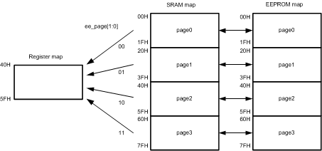 Figure 31. EEPROM Memory
EEPROM content is copied into SRAM always when the chip is taken from stand-by mode to active mode. Copying to SRAM can also be made during operation by writing the <ee_read> bit high and low in the EEPROM control (0DH) register. For reading the data from the SRAM, the page number must be set with <ee_page[1:0]> bits and the page read from addresses 40H – 5FH.
The EEPROM must be erased before programming. The erase command erases one page at time, which must be selected with <ee_page[1:0]> bits. This operation starts after setting and resetting <ee_erase> and takes about 100 ms after rising <ee_erase> bit. During erasing <ee_prog> bit of the EEPROM_CONTROL register is low. Corresponding SRAM area is erased with this operation also. <ee_erase> and <ee_prog> can be set only one command at a time (erase or program).
During programming the content of SRAM is copied to EEPROM, EEPROM programming cycle has two steps. At first, write the whole content of the SRAM, all 4 pages. The whole page can be written during one SPI/I2C cycle in the auto-increment mode. Second step is programming the EEPROM. This operation starts after writing <ee_prog> high and back low and takes about 100 ms after rising <ee_prog> bit. During programming <ee_prog> bit of the EEPROM_CONTROL register is low. For EEPROM erasing and programming the chip has to be in active mode (<NSTBY> high), the boost must be off (<in_boost> low) and the boost voltage set to 18 V (boost output register value 12H).
7.6 Register Maps
7.6.1 LP5520 Registers, Control Bits, and Default Values
All registers have their default value after power-on or reset. Default value for correction registers is 1000 0000 (multiplier = 1). Default value for adaptive voltage control and fast PWM is on. Default value for current set registers is 55H which sets the current to 20 mA. Default value for all other register bits is 0. Note that in automatic compensation mode the LED currents are obtained from the EEPROM.
Bits with r/o are read-only bits.
| ADR | REG NAME | D7 | D6 | D5 | D4 | D3 | D2 | D1 | D0 | DEFAULT |
| 00H | rgb
control |
seq_ mode[1] |
seq_ mode[0] |
en_fade | pwm_ fast |
rgb_auto | en_b | en_g | en_r | 0001 0000 |
| 01H | current
control (R) |
cc_r[7] | cc_r[6] | cc_r[5] | cc_r[4] | cc_r[3] | cc_r[2] | cc_r[1] | cc_r[0] | 0101 0101 |
| 02H | current
control (G) |
cc_g[7] | cc_g[6] | cc_g[5] | cc_g[4] | cc_g[3] | cc_g[2] | cc_g[1] | cc_g[0] | 0101 0101 |
| 03H | current
control (B) |
cc_b[7] | cc_b[6] | cc_b[5] | cc_b[4] | cc_b[3] | cc_b[2] | cc_b[1] | cc_b[0] | 0101 0101 |
| 04H | pwm brightness | brc_off | bri2 | bri1 | bri0 | 0000 0000 | ||||
| 05H | boost output | vprog[4] | vprog[3] | vprog[2] | vprog[1] | vprog[0] | 0000 0000 | |||
| 06H | control | adc_ch | comp_ sel |
en_ autoload |
vout_ auto |
en_boost | nstby | 0000 0100 | ||
| 08H | ADC_
hi_byte |
bit11 (r/o) |
bit10 (r/o) |
bit9 (r/o) |
bit8 (r/o) |
|||||
| 09H | ADC_
low_byte |
bit7 (r/o) |
bit6 (r/o) |
bit5 (r/o) |
bit4 (r/o) |
bit3 (r/o) |
bit2 (r/o) |
bit1 (r/o) |
bit0 (r/o) |
|
| 0AH | R correction | corr_r[7] | corr_r[6] | corr_r[5] | corr_r[4] | corr_r[3] | corr_r[2] | corr_r[1] | corr_r[0] | 1000 0000 |
| 0BH | G correction | corr_g[7] | corr_g[6] | corr_g[5] | corr_g[4] | corr_g[3] | corr_g[2] | corr_g[1] | corr_g[0] | 1000 0000 |
| 0CH | B correction | corr_b[7] | corr_b[6] | corr_b[5] | corr_b[4] | corr_b[3] | corr_b[2] | corr_b[1] | corr_b[0] | 1000 0000 |
| 0DH | EEPROM Control | ee_ready (r/o) |
ee_erase | ee_prog | ee_read | ee_page[1] | ee_page[0] | 0000 0000 |
Register addresses from 40H to 5FH contain the EEPROM page. EEPROM access is described in the Calibration Memory chapter.
7.6.1.1 Register Bit Conventions
Each register is shown with a key indicating the accessibility of the each individual bit, and the initial condition:
Table 13. Register Bit Accessibility And Initial Condition
| Key | Bit Accessibility |
| rw | Read/write |
| r | Read only |
| –0, –1 | Condition after POR |
rgb_control (00H) – RGB LEDs Control Register
| 7 | 6 | 5 | 4 | 3 | 2 | 1 | 0 |
| seq_mode1 | seq_mode0 | en_fade | pwm_fast | rgb_auto | en_b | en_g | en_r |
| rw-0 | rw-0 | rw-0 | rw-1 | rw-0 | rw-0 | rw-0 | rw-0 |
| seq_mode[1:0] | Bits 6 - 7 | 0 0 – overlapping PWM mode 0 1 – sequential mode with 2 PWM pulses 1 0 – sequential mode with 3 PWM pulses 1 1 – sequential mode with 4 PWM pulses |
| en_fade | Bit 5 | 0 – automatic fade disabled 1 – automatic fade enabled |
| pwm_fast | Bit 4 | 0 – normal PWM frequency 1.22 kHz 1 – high PWM frequency 19.52 kHz |
| rgb_auto | Bit 3 | 0 – automatic compensation disabled 1 – automatic compensation enabled |
| en_b | Bit 2 | 0 – blue LED output BOUT disabled 1 – blue LED output BOUT enabled |
| en_g | Bit 1 | 0 – green LED output GOUT disabled 1 – green LED output GOUT enabled |
| en_r | Bit 0 | 0 – red LED output ROUT disabled 1 – red LED output ROUT enabled |
current_control_R (01H) – Red LED Current Control Register
| 7 | 6 | 5 | 4 | 3 | 2 | 1 | 0 |
| cc_r[7] | cc_r[6] | cc_r[5] | cc_r[4] | cc_r[3] | cc_r[2] | cc_r[1] | cc_r[0] |
| rw-0 | rw-1 | rw-0 | rw-1 | rw-0 | rw-1 | rw-0 | rw-1 |
| cc_r[7:0] | Bits 7 - 0 | Adjustment | |
| cc_r[7:0] | Typical driver current (mA) | ||
| 0000 0000 | 0 | ||
| 0000 0001 | 0.234 | ||
| 0000 0010 | 0.468 | ||
| 0000 0011 | 0.702 | ||
| ... | ... | ||
| 1111 1101 | 59.202 | ||
| 1111 1110 | 59.436 | ||
| 1111 1111 | 59.670 | ||
current_control_G (02H) – Green LED Current Control Register
| 7 | 6 | 5 | 4 | 3 | 2 | 1 | 0 |
| cc_g[7] | cc_g[6] | cc_g[5] | cc_g[4] | cc_g[3] | cc_g[2] | cc_g[1] | cc_g[0] |
| rw-0 | rw-1 | rw-0 | rw-1 | rw-0 | rw-1 | rw-0 | rw-1 |
current_control_B (03H) – Blue LED Current Control Register
| 7 | 6 | 5 | 4 | 3 | 2 | 1 | 0 |
| cc_b[7] | cc_b[6] | cc_b[5] | cc_b[4] | cc_b[3] | cc_b[2] | cc_b[1] | cc_b[0] |
| rw-0 | rw-1 | rw-0 | rw-1 | rw-0 | rw-1 | rw-0 | rw-1 |
pwm_brightness (04H) – Brightness Control Register
| 7 | 6 | 5 | 4 | 3 | 2 | 1 | 0 |
| brc_off | bri[2] | bri[1] | bri[0] | ||||
| r-0 | r-0 | r-0 | rw-0 | r-0 | rw-0 | rw-0 | rw-0 |
| brc_off
bri[2:0] |
Bit 4 Bits 2-0 |
brc_off = 0 - stand-alone mode,
brightness is defined with external BRC signal |
||
| brc_off = 1 - brightness is defined with bri[2:0] | ||||
| Control | Multiplier | Intensity % | ||
| 0 | 0.008 | 0.8 | ||
| 1 | 0.016 | 1.6 | ||
| 10 | 0.031 | 3.1 | ||
| 11 | 0.063 | 6.3 | ||
| 100 | 0.125 | 12.5 | ||
| 101 | 0.250 | 25 | ||
| 110 | 0.500 | 50 | ||
| 111 | 1.000 | 100 | ||
boost_output (05H) – Boost Output Voltage Control Register
| 7 | 6 | 5 | 4 | 3 | 2 | 1 | 0 |
| vprog[4] | vprog[3] | vprog[2] | vprog[1] | vprog[0] | |||
| r-0 | r-0 | r-0 | r-0 | rw-0 | rw-0 | rw-0 | rw-0 |
| vprog[4:0] | Bits 4 - 0 | Adjustment | |
| vprog[4:0] | Typical boost output voltage (V) | ||
| 00101 | 5.0 | ||
| 00110 | 6.0 | ||
| 00111 | 7.0 | ||
| 01000 | 8.0 | ||
| 01001 | 9.0 | ||
| 01010 | 10.0 | ||
| 01011 | 11.0 | ||
| 01100 | 12.0 | ||
| 01101 | 13.0 | ||
| 01110 | 14.0 | ||
| 01111 | 15.0 | ||
| 10000 | 16.0 | ||
| 10001 | 17.0 | ||
| 10010 | 18.0 | ||
| 10011 | 19.0 | ||
| 10100 | 20.0 | ||
control (06H) – Control Register
| 7 | 6 | 5 | 4 | 3 | 2 | 1 | 0 |
| adc_ch | comp_sel | en_autoload | vout_auto | en_boost | nstby | ||
| r-0 | r-0 | rw-0 | rw-0 | rw-0 | rw-1 | rw-0 | rw-0 |
| adc_ch | Bit 5 | 0 – compensation depends from the external LM20 temperature sensor 1 – compensation depends from forward voltage of the red LED as temperature sensor |
| comp_sel | Bit 4 | 0 – compensation based on S1_IN input 1 – compensation based on S2_IN input |
| en_autoload | Bit 3 | 0 – internal boost converter loader off 1 – internal boost converter loader off |
| vout_auto | Bit 2 | 0 – manual boost output adjustment with boost_output register 1 – automatic adaptive boost output adjustment |
| en_boost | Bit 1 | 0 – boost converter disabled 1 – boost converter enabled |
| nstby | Bit 0 | 0 – LP5520 standby mode 1 – LP5520 active mode |
ADC_hi_byte (08H) – Analog Digital Converter Output, bits 8-11
| 7 | 6 | 5 | 4 | 3 | 2 | 1 | 0 |
| adc[11] | adc[10] | adc[9] | adc[8] | ||||
| r-0 | r-0 | r-0 | r-0 | r-0 | r-0 | r-0 | r-0 |
ADC_low_byte (09H) – Analog Digital Converter Output, bits 0-7
| 7 | 6 | 5 | 4 | 3 | 2 | 1 | 0 |
| adc[7] | adc[6] | adc[5] | adc[4] | adc[3] | adc[2] | adc[1] | adc[0] |
| r-0 | r-0 | r-0 | r-0 | r-0 | r-0 | r-0 | r-0 |
r_correction (0AH) – Additional Brightness Correction Value Register for Red LED
| 7 | 6 | 5 | 4 | 3 | 2 | 1 | 0 |
| corr_r[7] | corr_r[6] | corr_r[5] | corr_r[4] | corr_r[3] | corr_r[2] | corr_r[1] | corr_r[0] |
| rw-1 | rw-0 | rw-0 | rw-0 | rw-0 | rw-0 | rw-0 | rw-0 |
| corr_r[7:0] | Bits 7-0 | Correction | |
| corr_r[7:0] | Multiplier | ||
| 0000 0000 | 0 | ||
| 0000 0001 | 0.0078 | ||
| 0000 0010 | 0.0156 | ||
| ... | ... | ||
| 1000 0000 | 1.000 | ||
| ... | ... | ||
| 1111 1101 | 1.991 | ||
| 1111 1110 | 1.999 | ||
| 1111 1111 | 2.000 | ||
g_correction (0BH) – Additional Brightness Correction Value Register for Green LED
| 7 | 6 | 5 | 4 | 3 | 2 | 1 | 0 |
| corr_g[7] | corr_g[6] | corr_g[5] | corr_g[4] | corr_g[3] | corr_g[2] | corr_g[1] | corr_g[0] |
| rw-1 | rw-0 | rw-0 | rw-0 | rw-0 | rw-0 | rw-0 | rw-0 |
b_correction (0CH) – Additional Brightness Correction Value Register for Blue LED
| 7 | 6 | 5 | 4 | 3 | 2 | 1 | 0 |
| corr_b[7] | corr_b[6] | corr_b[5] | corr_b[4] | corr_b[3] | corr_b[2] | corr_b[1] | corr_b[0] |
| rw-1 | rw-0 | rw-0 | rw-0 | rw-0 | rw-0 | rw-0 | rw-0 |
EEPROM_control (0DH) – EEPROM Control Register
| 7 | 6 | 5 | 4 | 3 | 2 | 1 | 0 |
| ee_ready | ee_erase | ee_prog | ee_read | ee_page[1] | ee_page[0] | ||
| r-1 | rw-0 | rw-0 | r-0 | r-0 | r-0 | rw-0 | rw-0 |
| ee_ready | Bit 7 | EEPROM operations ready bit (read only) | |||
| ee_erase | Bit 6 | Start bit for erasing sequence | |||
| ee_prog | Bit 5 | Start bit for programming sequence | |||
| ee_read | Bit 4 | Read EEPROM data to SRAM | |||
| ee_page[1:0] | Bits 1-0 | ee_page[1] | ee_page[0] | page | EEPROM addresses |
| 0 | 0 | 0 | 00H-1FH (0-31) | ||
| 0 | 1 | 1 | 20H-3FH (32-63) | ||
| 1 | 0 | 2 | 40H-5FH (64-95) | ||
| 1 | 1 | 4 | 60H-7FH (96-127) | ||