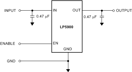
The LP5900 is an LDO capable of supplying 150-mA output current. Designed to meet the requirements of RF and analog circuits, the LP5900 device provides low noise, high PSRR, low quiescent current, and low line transient response figures. Using new innovative design techniques the LP5900 offers class-leading device noise performance without a noise bypass capacitor.
The device is designed to work with 0.47-μF input and output ceramic capacitors (no bypass capacitor required).
The device is available in a DSBGA (YZR) package and a WSON package; the device is also available in an extremely thin DSBGA (YPF) package. For all voltage and package options available today, see the Package Option Addendum (POA) at the end of this data sheet. For any other fixed output voltages from 1.5 V to 4.5 V in 25-mV steps and all other package options, contact your local TI Sales office.
PART NUMBER | PACKAGE | BODY SIZE |
---|---|---|
LP5900 | DSBGA (4) | 1.108 mm × 1.083 mm (MAX) |
WSON (6) | 2.50 mm × 2.20 mm (NOM) |
Changes from Q Revision (February 2015) to R Revision
Changes from P Revision (December 2014) to Q Revision
Changes from O Revision (April 2013) to P Revision
Changes from N Revision (April 2013) to O Revision
PIN | TYPE | DESCRIPTION | ||
---|---|---|---|---|
DSBGA | WSON | NAME | ||
A1 | 4 | EN | I | Enable input; disables the regulator when ≤ 0.4 V. Enables the regulator when ≥ 1.2 V. An internal 1-MΩ pull-down resistor connects this input to ground. |
A2 | 6 | IN | I | Input voltage supply. Connect a 0.47-µF capacitor at this input. |
B1 | 3 | GND | — | Common ground |
B2 | 1 | OUT | O | Output voltage. A 0.47-μF Low ESR capacitor should be connected to this pin. Connect this output to the load circuit. |
— | 2 | NC | — | No internal connection. |
— | Thermal Pad | Thermal Pad | — | The exposed thermal pad on the bottom of the packagemust be connected to a copper area on the PCB under the package. TI recommends use of thermal vias to remove heat from the package into the PCB. Connect the thermal pad to ground potential or leave floating. Do not connect the thermal pad to any potential other than the same ground potential seen at device pin 3. For additional information on using TI's non-pullback WSON package, see AN-1187 Leadless Leadframe Package (LLP) (SNOA401). |
MIN | MAX | UNIT | |
---|---|---|---|
Input voltage, VIN | –0.3 | 6 | V |
Output voltage, VOUT | –0.3 | VIN + 0.3 | |
Enable input voltage, VEN | –0.3 | VIN + 0.3 | |
Continuous power dissipation(4) | Internally Limited | ||
Junction temperature, TJMAX | 150 | °C | |
Storage temperature, Tstg | –65 | 150 | °C |
VALUE | UNIT | |||
---|---|---|---|---|
V(ESD) | Electrostatic discharge | Human-body model (HBM), per ANSI/ESDA/JEDEC JS-001(1) | ±2000 | V |
MIN | MAX | UNIT | |
---|---|---|---|
Input voltage, VIN | 2.5 | 5.5 | V |
Enable voltage, VEN | 0 | VIN + 0.3 | V |
Output current, IOUT(2) | 0 | 150 | mA |
Junction temperature, TJ | –40 | 125 | °C |
Ambient temperature, TA(2) | –40 | 85 | °C |
THERMAL METRIC(1) | LP5900 | UNIT | ||
---|---|---|---|---|
NGF | YZR/YPF | |||
6 PINS | 4 PINS | |||
RθJA | Junction-to-ambient thermal resistance | 79.8 | 177.7 | °C/W |
RθJC(top) | Junction-to-case (top) thermal resistance | 84.4 | 0.7 | °C/W |
RθJB | Junction-to-board thermal resistance | 20.4 | 35.6 | °C/W |
ψJT | Junction-to-top characterization parameter | 2.6 | 5.8 | °C/W |
ψJB | Junction-to-board characterization parameter | 20.3 | 35.3 | °C/W |
RθJC(bot) | Junction-to-case (bottom) thermal resistance | 11.2 | — | °C/W |
PARAMETER | TEST CONDITIONS | MIN | TYP | MAX | UNIT | ||
---|---|---|---|---|---|---|---|
VIN | Input voltage | 2.5 | 5.5 | V | |||
ΔVOUT | Output voltage tolerance | VIN = (VOUT(NOM) + 1 V) to 5.5 V, IOUT = 1 mA to 150 mA, –40°C ≤ TJ ≤ 125°C |
−2% | 2% | |||
Line regulation | VIN = (VOUT(NOM) + 1 V) to 5.5 V, IOUT = 1 mA | 0.05 | %V | ||||
Load regulation | IOUT = 1 mA to 150 mA | 0.001 | %mA | ||||
ILOAD | Load current | See(3) | mA | ||||
Maximum output current | –40°C ≤ TJ ≤ 125°C | 150 | |||||
IQ | Quiescent current(4) | VEN = 1.2 V, IOUT = 0 mA | 25 | µA | |||
VEN = 1.2 V, IOUT = 0 mA, –40°C ≤ TJ ≤ 125°C | 50 | ||||||
VEN = 1.2 V, IOUT = 150 mA | 160 | ||||||
VEN = 1.2 V, IOUT = 150 mA, –40°C ≤ TJ ≤ 125°C | 230 | ||||||
VEN = 0.3 V (disabled) | 0.003 | ||||||
VEN = 0.3 V (disabled, –40°C ≤ TJ ≤ 125°C | 1 | ||||||
IG | Ground current(5) | IOUT = 0 mA (VOUT = 2.5 V) | 30 | µA | |||
VDO | Dropout voltage(6) | IOUT = 150 mA | 80 | mV | |||
IOUT = 150 mA, –40°C ≤ TJ ≤ 125°C | 150 | ||||||
ISC | Short-circuit current limit(7) | 300 | mA | ||||
PSRR | Power supply rejection ratio(8) | f = 100 Hz, IOUT = 150 mA | 85 | dB | |||
f = 1 kHz, IOUT = 150 mA | 75 | ||||||
f = 10 kHz, IOUT = 150 mA | 65 | ||||||
f = 50 kHz, IOUT = 150 mA | 52 | ||||||
f = 100 kHz, IOUT = 150 mA | 40 | ||||||
en | Output noise voltage(8) | BW = 10 Hz to 100 kHz, VIN = 4.2 V | IOUT = 0 mA | 7 | μVRMS | ||
IOUT = 1 mA | 10 | ||||||
IOUT = 150 mA | 6.5 | ||||||
TSHUTDOWN | Thermal shutdown | Temperature | 160 | ºC | |||
Hysteresis | 20 | ||||||
LOGIN INPUT THRESHOLDS | |||||||
VIL | Low input threshold (VEN) | VIN = 2.5 V to 5.5 V, –40°C ≤ TJ ≤ 125°C | 0.4 | V | |||
VIH | High input threshold (VEN) | VIN = 2.5 V to 5.5 V, –40°C ≤ TJ ≤ 125°C | 1.2 | V | |||
IEN | Input current at EN pin(9) | VEN = 5.5 V and VIN = 5.5 V | 5.5 | μA | |||
VEN = 0 V and VIN = 5.5 V | 0.001 | ||||||
TRANSIENT CHARACTERISTICS | |||||||
ΔVOUT | Line transient(8) | VIN = (VOUT(NOM) + 1 V) to (VOUT(NOM) + 1.6 V) in 30 μs, IOUT = 1 mA, –40°C ≤ TJ ≤ 125°C | −2 | mV | |||
VIN = (VOUT(NOM) + 1.6 V) to (VOUT(NOM) + 1 V) in 30 μs, IOUT = 1 mA, –40°C ≤ TJ ≤ 125°C | 2 | ||||||
Load transient(8) | IOUT = 1 mA to 150 mA in 10 μs, –40°C ≤ TJ ≤ 125°C | −110 | mV | ||||
IOUT = 150 mA to 1 mA in 10 μs, –40°C ≤ TJ ≤ 125°C | 50 | ||||||
Overshoot on start-up(8) | –40°C ≤ TJ ≤ 125°C | 20 | mV | ||||
Turnon time | To 95% of VOUT(NOM) | 150 | 300 | μs |
PARAMETER | TEST CONDITIONS | MIN | NOM | MAX | UNIT | |
---|---|---|---|---|---|---|
CIN | Input capacitance | Capacitance for stability | 0.47 | µF | ||
Capacitance for stability, –40°C ≤ TJ ≤ 125°C | 0.33 | |||||
COUT | Output capacitance | Capacitance for stability | 0.47 | |||
Capacitance for stability, –40°C ≤ TJ ≤ 125°C | 0.33 | 10 | ||||
ESR | Output/Input capacitance | 5 | 500 | mΩ |
Designed to meet the needs of sensitive RF and analog circuits, the LP5900 provides low noise, high PSRR, and low quiescent current, as well as low line and load transient response figures. Using new innovative design techniques, the LP5900 offers class-leading noise performance without the need for a separate noise filter capacitor.
The LP5900 remains stable and in regulation with no external load.
The LP5900 enable (EN) pin is internally held low by a 1-MΩ resistor to GND. The EN must be higher than the VIH threshold to ensure that the device is fully enabled under all operating conditions. The EN pin voltage must be lower than the VIL threshold to ensure that the device is fully disabled.
Any internal noise at the LP5900 reference voltage is reduced by a first order low-pass RC filter before it is passed to the output buffer stage. This eliminates the need for the external bypass capacitor for noise suppression.
Thermal-overload protection disables the output when the junction temperature rises to approximately 160°C which allows the device to cool. When the junction temperature cools to approximately 140°C, the output is enabled. Based on power dissipation, thermal resistance, and ambient temperature, the thermal protection circuit may cycle on and off. This thermal cycling limits the dissipation of the regulator and protects it from damage as a result of overheating.
The LP5900 may be switched ON or OFF by a logic input at the EN pin. A high voltage at this pin turns the device on. When the EN pin is low, the regulator output is off, and the device typically consumes 3 nA. However, if the application does not require the shutdown feature, the EN pin can be tied to IN pin to keep the regulator output permanently on. In this case the supply voltage must be fully established 500 μs or less to ensure correct operation of the start-up circuit. Failure to comply with this condition may cause a delayed start-up time of several seconds.
A 1 MΩ pull-down resistor ties the EN input to ground, and this ensures that the device will remain off when the EN pin is left open circuit. To ensure proper operation, the signal source used to drive the EN input must be able to swing above and below the specified turn-on/off voltage thresholds listed in the Electrical Characteristics section under VIL and VIH.
The LP5900 does not include any dedicated UVLO circuitry. The LP5900 internal circuitry is not fully functional until VIN is at least 2.5 V. The output voltage is not regulated until VIN ≥ (VOUT + VDO).