SNVS358R July 2005 – June 2016 LP5900
PRODUCTION DATA.
- 1 Features
- 2 Applications
- 3 Description
- 4 Revision History
- 5 Pin Configuration and Functions
- 6 Specifications
- 7 Detailed Description
- 8 Application and Implementation
- 9 Power Supply Recommendations
- 10Layout
- 11Device and Documentation Support
- 12Mechanical, Packaging, and Orderable Information
パッケージ・オプション
メカニカル・データ(パッケージ|ピン)
サーマルパッド・メカニカル・データ
発注情報
10 Layout
10.1 Layout Guidelines
The device is designed to operate from an input voltage supply range between 2.5 V and 5.5 V. This input supply must be well regulated. To ensure that the LP5900 output voltage is well regulated, the input supply must be at least VOUT + 1 V.
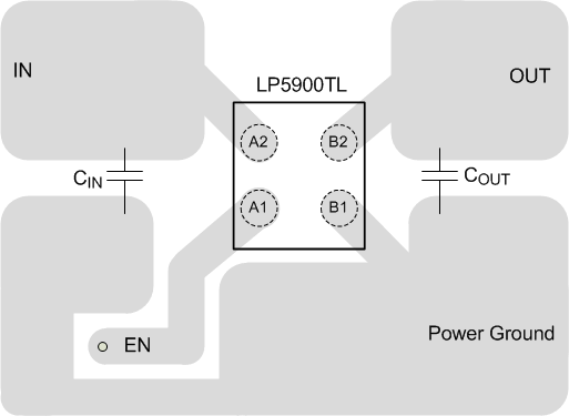
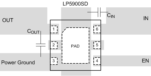
10.2 Layout Examples
 Figure 18. DSBGA Layout
 Figure 19. WSON Layout
10.3 DSBGA Mounting
The DSBGA package requires specific mounting techniques, which are detailed in AN-1112 DSBGA Wafer Level Chip Scale Package (SNVA009). For best results during assembly, alignment ordinals on the PC board may be used to facilitate placement of the DSBGA device.
For best results during assembly, alignment ordinals on the PC board may be used to facilitate placement of the DSBGA device.
10.4 DSBGA Light Sensitivity
Exposing the DSBGA device to direct light may cause incorrect operation of the device. Light sources such as halogen lamps can affect electrical performance if they are situated in proximity to the device.
Light with wavelengths in the red and infra-red part of the spectrum has the most detrimental effect; thus, the fluorescent lighting used inside most buildings has very little effect on performance.
10.5 WSON Mounting
The 6-lead WSON package requires specific mounting techniques which are detailed in AN-1187 Leadless Leadframe Package (LLP) (SNOA401). Referring to the section PCB Design Recommendations, it should be noted that the pad style which should be used with the WSON package is the NSMD (non-solder mask defined) type. Additionally, it is recommended the PCB terminal pads to be 0.2 mm longer than the package pads to create a solder fillet to improve reliability and inspection.
The exposed thermal pad on the bottom of the WSON package must be connected to a copper area on the PCB under the package. TI recommends use of thermal vias to remove heat from the package into the PCB is recommended. Connect the thermal pad to ground potential or leave floating. Do not connect the thermal pad to any potential other than the same ground potential seen at device pin 3.