JAJSCR1 November 2016 LP5922
PRODUCTION DATA.
- 1 特長
- 2 アプリケーション
- 3 概要
- 4 改訂履歴
- 5 Pin Configuration and Functions
- 6 Specifications
- 7 Detailed Description
-
8 Applications and Implementation
- 8.1 Application Information
- 8.2
Typical Application
- 8.2.1 Design Requirements
- 8.2.2
Detailed Design Procedure
- 8.2.2.1 External Capacitors
- 8.2.2.2 Input Capacitor, CIN
- 8.2.2.3 Output Capacitor, COUT
- 8.2.2.4 Soft-Start and Noise-Reduction Capacitor, CSS/NR
- 8.2.2.5 Feed-Forward Capacitor, CFF
- 8.2.2.6 No-Load Stability
- 8.2.2.7 Power Dissipation
- 8.2.2.8 Estimating Junction Temperature
- 8.2.2.9 Recommended Continuous Operating Area
- 8.2.3 Application Curves
- 9 Power Supply Recommendations
- 10Layout
- 11デバイスおよびドキュメントのサポート
- 12メカニカル、パッケージ、および注文情報
8 Applications and Implementation
NOTE
Information in the following applications sections is not part of the TI component specification, and TI does not warrant its accuracy or completeness. TI’s customers are responsible for determining suitability of components for their purposes. Customers should validate and test their design implementation to confirm system functionality.
8.1 Application Information
The LP5922 is designed to meet the requirements of RF and analog circuits, by providing low noise, high PSRR, low quiescent current, and low line or load transient response figures. The device offers excellent noise performance without the need for a noise bypass capacitor and is stable with input and output capacitors with a value of 22 µF. The LP5922 delivers this performance in an industry-standard WSON package which, for this device, is specified with an operating junction temperature (TJ) of –40°C to +125°C.
8.2 Typical Application
Figure 15 shows the typical application circuit for the LP5922. Input and output capacitances may need to be increased above 22 µF minimum for some applications.
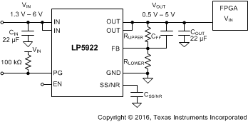 Figure 15. LP5922 Typical Application
8.2.1 Design Requirements
For typical LP5922 applications, use the parameters listed in Table 1.
Table 1. Design Parameters
| DESIGN PARAMETER | EXAMPLE VALUE |
|---|---|
| Input voltage | 2.25 V to 2.75 V |
| Output voltage | 1.8 V |
| Output current | 2000 mA |
| Output capacitor range | 22 µF to 47 µF |
| Output capacitor ESR range | 2 mΩ to 500 mΩ |
8.2.2 Detailed Design Procedure
8.2.2.1 External Capacitors
The LP5922 is designed to be stable using low equivalent series resistance (ESR) ceramic capacitors at the input, output, and the noise-reduction pin (SS/NR). Multilayer ceramic capacitors have become the industry standard for these types of applications and are recommended, but must be used with good judgment. Ceramic capacitors that employ X7R-, X5R-, and COG-rated dielectric materials provide relatively good capacitive stability across temperature, whereas the use of Y5V-rated capacitors is discouraged because of large variations in capacitance. Additionally, the case size has a direct impact on the capacitance versus applied voltage derating.
Regardless of the ceramic capacitor type selected, the actual capacitance varies with the applied operating voltage and temperature. As a rule of thumb, derate ceramic capacitors by at least 50%. The input and output capacitors recommended herein account for a effective capacitance derating of approximately 50%, but at high applied voltage conditions the capacitance derating can be greater than 50% and must be taken into consideration. The minimum capacitance values declared in Input and Output Capacitors must be met across the entire expected operating voltage range and temperature range.
8.2.2.2 Input Capacitor, CIN
An input capacitor is required for stability. A capacitor with a value of at least 22 μF must be connected between the LP5922 IN pin and ground for stable operation over full load current range. It is acceptable to have more output capacitance than input, as long as the input is at least 22 μF.
The input capacitor must be located as close as possible to, but at a distance not more than 1 cm from, the IN pin and returned to the device GND pin with a clean analog ground. This will minimize the trace inductance between the capacitor and the device. Any good quality ceramic or tantalum capacitor may be used at the input.
8.2.2.3 Output Capacitor, COUT
The LP5922 is designed to work specifically with a low ESR ceramic (MLCC) output capacitor, typically 22 μF. A ceramic capacitor (dielectric types X5R or X7R) in the 22-μF to 100-μF range, with an ESR not exceeding 500 mΩ, is suitable in the LP5922 application circuit having an output voltage greater than 0.8 V. For output voltages of 0.8 V or less, the output capacitance must be increased to typically 47 μF. The output capacitor must be connected between the device OUT and GND pins. The output capacitor must meet the requirement for the minimum value of capacitance and have an ESR value that does not exceed 500 mΩ to ensure stability.
It is possible to use tantalum capacitors at the device output, but these are not as attractive for reasons of size, cost, and performance.
A combination of multiple output capacitors in parallel boosts the high-frequency PSRR. The combination of one 0805-sized, 47-µF ceramic capacitor in parallel with two 0805-sized, 10-µF ceramic capacitors with a sufficient voltage rating optimizes PSRR response in the frequency range of 400 kHz to 700 kHz (which is a typical range for dc-dc supply switching frequency). This 47-µF || 10-µF || 10-µF combination also ensures that at high input voltage and high output voltage configurations, the minimum effective capacitance is met. Many 0805-sized, 47-µF ceramic capacitors have a voltage derating of approximately 60% to 75% at 5 V, so the addition of the two 10-µF capacitors ensures that the capacitance is at or above 22 µF.
8.2.2.4 Soft-Start and Noise-Reduction Capacitor, CSS/NR
Recommended value for CSS/NR is 100 nF or larger. The soft-start period can be calculated by Equation 2. The CSS/NR capacitor is also the filter capacitor for internal reference for noise reduction purpose.
8.2.2.5 Feed-Forward Capacitor, CFF
Although a feed-forward capacitor (CFF) from the FB pin to the OUT pin is not required to achieve stability, a 10-nF external CFF optimizes the transient, noise, and PSRR performance. A higher capacitance CFF value can be used; however, the start-up time may be longer and the Power-Good signal may incorrectly indicate that the output voltage is settled. The maximum recommended value is 100 nF
To ensure proper PGx functionality, the time constant defined by CNR/SSx must be greater than or equal to the time constant from CFFx. For a detailed description, see the application report Pros and Cons of Using a Feed-Forward Capacitor with a Low Dropout Regulator (SBVA042).
8.2.2.6 No-Load Stability
The LP5922 remains stable, and in regulation, with no external load.
8.2.2.7 Power Dissipation
Knowing the device power dissipation and proper sizing of the thermal plane connected to the exposed thermal pad is critical to ensuring reliable operation. Device power dissipation depends on input voltage, output voltage, and load conditions and can be calculated with Equation 3.
Power dissipation can be minimized, and greater efficiency can be achieved, by using the lowest available voltage drop option that is greater than the dropout voltage (VDO). However, keep in mind that higher voltage drops result in better dynamic (that is, PSRR and transient) performance.
On the WSON (DSC) package, the primary conduction path for heat is through the exposed thermal pad into the PCB. To ensure the device does not overheat, connect the exposed thermal pad, through multiple thermal vias, to an internal ground plane with an appropriate amount of PCB copper area.
Power dissipation and junction temperature are most often related by the junction-to-ambient thermal resistance (RθJA) of the combined PCB and device package and the temperature of the ambient air (TA), according to Equation 4 or Equation 5:
If the VIN-VOUT voltage is known, the maximum allowable output current can be calculated with Equation 6
Unfortunately, the RθJA value is highly dependent on the heat-spreading capability of the particular PCB design, and therefore varies according to the PCB size, total copper area, copper weight, any thermal vias, and location of the planes. The RθJA recorded in Thermal Information is determined by the specific EIA/JEDEC JESD51-7 standard for PCB and copper spreading area, and is to be used only as a relative measure of package thermal performance. For a well designed thermal layout, RθJA is actually the sum of the package junction-to-case (bottom) thermal resistance (RθJC(bot)) plus the thermal resistance contribution by the PCB copper area acting as a heat sink.
8.2.2.8 Estimating Junction Temperature
The JEDEC standard now recommends the use of psi (Ψ) thermal metrics to estimate the junction temperatures of the LDO when in-circuit on a typical PCB board application. These metrics are not strictly speaking thermal resistances, but rather offer practical and relative means of estimating junction temperatures. These psi metrics are determined to be significantly independent of the copper-spreading area. The key thermal metrics (ΨJT and ΨJB) are given in the Thermal Information table and are used in accordance with Equation 7 and Equation 8.
where
- TTOP is the temperature measured at the center-top of the device package.
- PD(MAX) is described at Equation 3
where
- TBOARD is the PCB surface temperature measured 1 mm from the device package and centered on the package edge.
- PD(MAX) is described at Equation 3
For more information about the thermal characteristics ΨJT and ΨJB, see Semiconductor and IC Package Thermal Metrics ; for more information about measuring TTOP and TBOARD, see Using New Thermal Metrics ; and for more information about the EIA/JEDEC JESD51 PCB used for validating RθJA, see the TI Application Report Thermal Characteristics of Linear and Logic Packages Using JEDEC PCB Designs. These application notes are available at www.ti.com.
8.2.2.9 Recommended Continuous Operating Area
The continuous operational area of an LDO is limited by the input voltage (VIN), the output voltage (VOUT), the dropout voltage (VDO), the output current (IOUT), and the junction temperature (TJ). The recommended area for continuous operation for a linear regulator can be separated into the following steps, and is shown in Figure 16.
- Limited by dropout: Dropout voltage limits the minimum differential voltage between the input and the output (VIN – VOUT) at a given output current level.
- Limited by the rated output current: The rated output current limits the maximum recommended output current level. Exceeding this rating causes the device to fall out of specification.
- Limited by thermals: This portion of the boundary is defined by Equation 6. The slope is nonlinear because the junction temperature of the LDO is controlled by the power dissipation (PD) across the LDO; therefore, when VIN – VOUT increases, the output current must decrease in order to ensure that the rated maximum operating junction temperature of the device is not exceeded. Exceeding the maximum operating junction temperature rating can cause the device to fall out of specifications, reduces long-term reliability, and may activate the thermal shutdown protection circuitry.
- Limited by VIN range: The rated operating input voltage range governs both the minimum and maximum of VIN – VOUT.
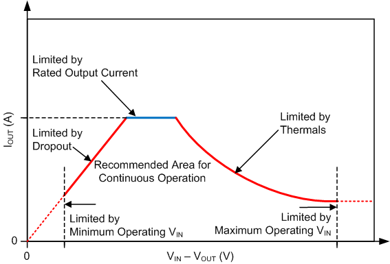 Figure 16. Recommended Continuous Operating Area
Figure 17 to Figure 22 show the recommended continuous operating area boundaries for this device in the WSON (DSC) package mounted to a EIA/JEDEC High-K printed circuit board, as defined by JESD51-7, with an RθJA rating of 49.5°C/W.
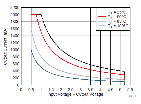 Figure 17. Recommended Continuous Operating Area for VOUT = 0.8 V
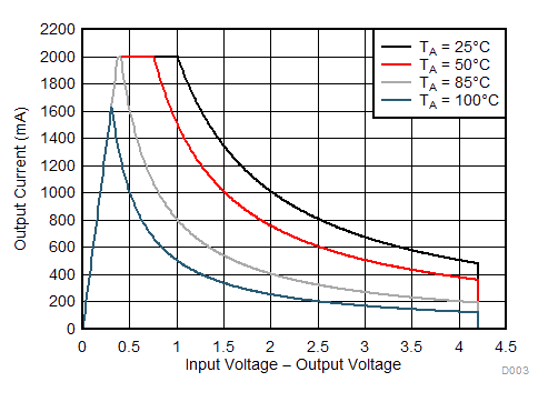 Figure 19. Recommended Continuous Operating Area for VOUT = 1.8 V
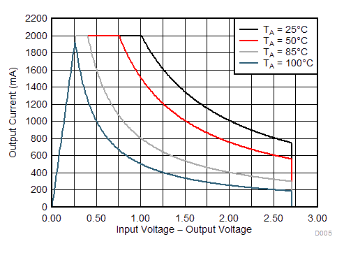 Figure 21. Recommended Continuous Operating Area for VOUT = 3.3 V
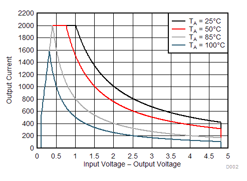 Figure 18. Recommended Continuous Operating Area for VOUT = 1.2 V
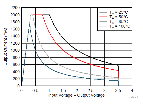 Figure 20. Recommended Continuous Operating Area for VOUT = 2.5 V
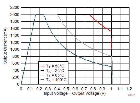 Figure 22. Recommended Continuous Operating Area for VOUT = 5 V
8.2.3 Application Curves
