SNVSB23 March 2018 LP87521-Q1 , LP87522-Q1 , LP87523-Q1 , LP87524-Q1 , LP87525-Q1
PRODUCTION DATA.
- 1 Features
- 2 Applications
- 3 Description
- 4 Revision History
- 5 Device Comparison Table
- 6 Pin Configuration and Functions
- 7 Specifications
-
8 Detailed Description
- 8.1 Overview
- 8.2 Functional Block Diagram
- 8.3
Feature Descriptions
- 8.3.1 Multi-Phase DC/DC Converters
- 8.3.2 Sync Clock Functionality
- 8.3.3 Power-Up
- 8.3.4 Regulator Control
- 8.3.5 Enable and Disable Sequences
- 8.3.6 Device Reset Scenarios
- 8.3.7 Diagnosis and Protection Features
- 8.3.8 GPIO Signal Operation
- 8.3.9 Digital Signal Filtering
- 8.4 Device Functional Modes
- 8.5 Programming
- 8.6
Register Maps
- 8.6.1
Register Descriptions
- 8.6.1.1 OTP_REV
- 8.6.1.2 BUCK0_CTRL1
- 8.6.1.3 BUCK1_CTRL1
- 8.6.1.4 BUCK2_CTRL1
- 8.6.1.5 BUCK3_CTRL1
- 8.6.1.6 BUCK0_VOUT
- 8.6.1.7 BUCK0_FLOOR_VOUT
- 8.6.1.8 BUCK1_VOUT
- 8.6.1.9 BUCK1_FLOOR_VOUT
- 8.6.1.10 BUCK2_VOUT
- 8.6.1.11 BUCK2_FLOOR_VOUT
- 8.6.1.12 BUCK3_VOUT
- 8.6.1.13 BUCK3_FLOOR_VOUT
- 8.6.1.14 BUCK0_DELAY
- 8.6.1.15 BUCK1_DELAY
- 8.6.1.16 BUCK2_DELAY
- 8.6.1.17 BUCK3_DELAY
- 8.6.1.18 GPIO2_DELAY
- 8.6.1.19 GPIO3_DELAY
- 8.6.1.20 RESET
- 8.6.1.21 CONFIG
- 8.6.1.22 INT_TOP1
- 8.6.1.23 INT_TOP2
- 8.6.1.24 INT_BUCK_0_1
- 8.6.1.25 INT_BUCK_2_3
- 8.6.1.26 TOP_STAT
- 8.6.1.27 BUCK_0_1_STAT
- 8.6.1.28 BUCK_2_3_STAT
- 8.6.1.29 TOP_MASK1
- 8.6.1.30 TOP_MASK2
- 8.6.1.31 BUCK_0_1_MASK
- 8.6.1.32 BUCK_2_3_MASK
- 8.6.1.33 SEL_I_LOAD
- 8.6.1.34 I_LOAD_2
- 8.6.1.35 I_LOAD_1
- 8.6.1.36 PGOOD_CTRL1
- 8.6.1.37 PGOOD_CTRL2
- 8.6.1.38 PGOOD_FLT
- 8.6.1.39 PLL_CTRL
- 8.6.1.40 PIN_FUNCTION
- 8.6.1.41 GPIO_CONFIG
- 8.6.1.42 GPIO_IN
- 8.6.1.43 GPIO_OUT
- 8.6.1
Register Descriptions
- 9 Application and Implementation
- 10Power Supply Recommendations
- 11Layout
- 12Device and Documentation Support
- 13Mechanical, Packaging, and Orderable Information
パッケージ・オプション
デバイスごとのパッケージ図は、PDF版データシートをご参照ください。
メカニカル・データ(パッケージ|ピン)
- RNF|26
サーマルパッド・メカニカル・データ
発注情報
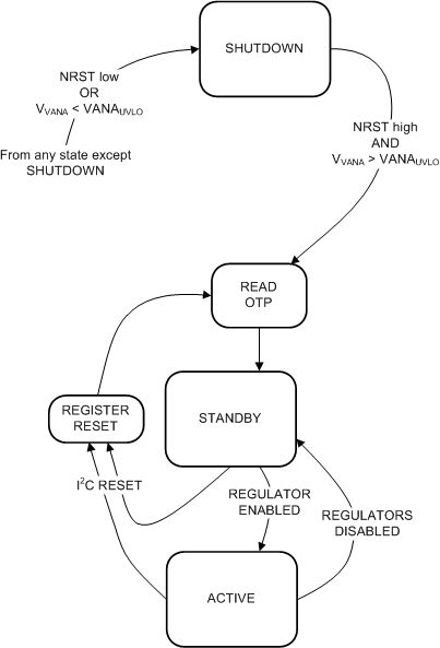
8.4.1 Modes of Operation
- SHUTDOWN:The NRST voltage is below threshold level. All switch, reference, control, and bias circuitry of the LP8752x-Q1 device are turned off.
- READ OTP:The primary supply voltage VANA is above VANAUVLO level, and NRST voltage is above threshold level. The regulators are disabled, and the reference and bias circuitry of the LP8752x-Q1 are enabled. The OTP bits are loaded to registers.
- STANDBY:The primary supply voltage VANA is above VANAUVLO level, and NRST voltage is above threshold level. The regulators are disabled, and the reference, control,and bias circuitry of the LP8752x-Q1 are enabled. All registers can be read or written by the host processor via the system serial interface. The regulators can be enabled if needed.
- ACTIVE:The primary supply voltage VANA is above VANAUVLO level, and NRST voltage is above threshold level. At least one regulated DC/DC converter is enabled. All registers can be read or written by the host processor via the system serial interface.
The operating modes and transitions between the modes are shown in Figure 21.
 Figure 21. Device Operation Modes