SNVSB23 March 2018 LP87521-Q1 , LP87522-Q1 , LP87523-Q1 , LP87524-Q1 , LP87525-Q1
PRODUCTION DATA.
- 1 Features
- 2 Applications
- 3 Description
- 4 Revision History
- 5 Device Comparison Table
- 6 Pin Configuration and Functions
- 7 Specifications
-
8 Detailed Description
- 8.1 Overview
- 8.2 Functional Block Diagram
- 8.3
Feature Descriptions
- 8.3.1 Multi-Phase DC/DC Converters
- 8.3.2 Sync Clock Functionality
- 8.3.3 Power-Up
- 8.3.4 Regulator Control
- 8.3.5 Enable and Disable Sequences
- 8.3.6 Device Reset Scenarios
- 8.3.7 Diagnosis and Protection Features
- 8.3.8 GPIO Signal Operation
- 8.3.9 Digital Signal Filtering
- 8.4 Device Functional Modes
- 8.5 Programming
- 8.6
Register Maps
- 8.6.1
Register Descriptions
- 8.6.1.1 OTP_REV
- 8.6.1.2 BUCK0_CTRL1
- 8.6.1.3 BUCK1_CTRL1
- 8.6.1.4 BUCK2_CTRL1
- 8.6.1.5 BUCK3_CTRL1
- 8.6.1.6 BUCK0_VOUT
- 8.6.1.7 BUCK0_FLOOR_VOUT
- 8.6.1.8 BUCK1_VOUT
- 8.6.1.9 BUCK1_FLOOR_VOUT
- 8.6.1.10 BUCK2_VOUT
- 8.6.1.11 BUCK2_FLOOR_VOUT
- 8.6.1.12 BUCK3_VOUT
- 8.6.1.13 BUCK3_FLOOR_VOUT
- 8.6.1.14 BUCK0_DELAY
- 8.6.1.15 BUCK1_DELAY
- 8.6.1.16 BUCK2_DELAY
- 8.6.1.17 BUCK3_DELAY
- 8.6.1.18 GPIO2_DELAY
- 8.6.1.19 GPIO3_DELAY
- 8.6.1.20 RESET
- 8.6.1.21 CONFIG
- 8.6.1.22 INT_TOP1
- 8.6.1.23 INT_TOP2
- 8.6.1.24 INT_BUCK_0_1
- 8.6.1.25 INT_BUCK_2_3
- 8.6.1.26 TOP_STAT
- 8.6.1.27 BUCK_0_1_STAT
- 8.6.1.28 BUCK_2_3_STAT
- 8.6.1.29 TOP_MASK1
- 8.6.1.30 TOP_MASK2
- 8.6.1.31 BUCK_0_1_MASK
- 8.6.1.32 BUCK_2_3_MASK
- 8.6.1.33 SEL_I_LOAD
- 8.6.1.34 I_LOAD_2
- 8.6.1.35 I_LOAD_1
- 8.6.1.36 PGOOD_CTRL1
- 8.6.1.37 PGOOD_CTRL2
- 8.6.1.38 PGOOD_FLT
- 8.6.1.39 PLL_CTRL
- 8.6.1.40 PIN_FUNCTION
- 8.6.1.41 GPIO_CONFIG
- 8.6.1.42 GPIO_IN
- 8.6.1.43 GPIO_OUT
- 8.6.1
Register Descriptions
- 9 Application and Implementation
- 10Power Supply Recommendations
- 11Layout
- 12Device and Documentation Support
- 13Mechanical, Packaging, and Orderable Information
パッケージ・オプション
デバイスごとのパッケージ図は、PDF版データシートをご参照ください。
メカニカル・データ(パッケージ|ピン)
- RNF|26
サーマルパッド・メカニカル・データ
発注情報
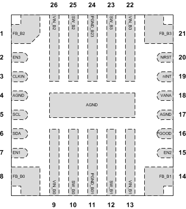
6 Pin Configuration and Functions
RNF Package
26-Pin VQFN-HR With Thermal Pad
Top View

Pin Functions
| PIN | TYPE(1) | DESCRIPTION | |
|---|---|---|---|
| NO. | NAME | ||
| 1 | FB_B2 | A | Output voltage feedback (positive) for the BUCK2 converter. |
| 2 | EN3 | D/I/O | Programmable enable signal for the buck regulators (can be also configured to select between two buck output-voltage levels). This pin functions alternatively as GPIO3. |
| 3 | CLKIN | D/I | External clock input. Connect this pin to ground if the external clock is not used. |
| 4, 17, Thermal Pad | AGND | G | Ground |
| 5 | SCL | D/I | Serial interface clock input for I2C access. Connect this pin to a pullup resistor. |
| 6 | SDA | D/I/O | Serial interface data input and output for I2C access. Connect this pin to a pullup resistor. |
| 7 | EN1 | D/I/O | Programmable enable signal for the buck regulators (can be also configured to select between two buck output voltage levels). This pin functions alternatively as GPIO1. |
| 8 | FB_B0 | A | Output voltage feedback (positive) for the BUCK0 converter. |
| 9 | VIN_B0 | P | Input for the BUCK0 converter. The separate power pins, VIN_Bx, are not connected together internally. The VIN_Bx pins must be connected together in the application and be locally bypassed. |
| 10 | SW_B0 | A | BUCK0 switch node |
| 11 | PGND_B01 | G | Power ground for the BUCK0 and BUCK1 converters |
| 12 | SW_B1 | A | BUCK1 switch node |
| 13 | VIN_B1 | P | Input for the BUCK1 converter. The separate power pins, VIN_Bx, are not connected together internally. The VIN_Bx pins must be connected together in the application and be locally bypassed. |
| 14 | FB_B1 | A | Output voltage feedback (positive) for the BUCK1 converter. This pin functions alternatively as the output ground feedback (negative) for the BUCK0 converter. |
| 15 | EN2 | D/I/O | Programmable enable signal for the buck regulators (can be also configured to select between two buck output voltage levels). This pin functions alternatively as GPIO2. |
| 16 | PGOOD | D/O | Power-good indication signal |
| 18 | VANA | P | Supply voltage for the analog and digital blocks. This pin must be connected to the same node as VIN_Bx. |
| 19 | nINT | D/O | Open-drain interrupt output. This pin is active low. |
| 20 | NRST | D/I | Reset signal for the device |
| 21 | FB_B3 | A | Output voltage feedback (positive) for the BUCK3 converter. This pin functions alternatively as the output ground feedback (negative) for the BUCK2 converter. |
| 22 | VIN_B3 | P | Input for the BUCK3 converter. The separate power pins, VIN_Bx, are not connected together internally. The VIN_Bx pins must be connected together in the application and be locally bypassed. |
| 23 | SW_B3 | A | BUCK3 switch node |
| 24 | PGND_B23 | G | Power ground for the BUCK2 and BUCK3 converters |
| 25 | SW_B2 | A | BUCK2 switch node |
| 26 | VIN_B2 | P | Input for the BUCK2 converter. The separate power pins, VIN_Bx, are not connected together internally. The VIN_Bx pins must be connected together in the application and be locally bypassed. |
(1) A: Analog Pin, D: Digital Pin, G: Ground Pin, P: Power Pin, I: Input Pin, O: Output Pin