SNVSB23 March 2018 LP87521-Q1 , LP87522-Q1 , LP87523-Q1 , LP87524-Q1 , LP87525-Q1
PRODUCTION DATA.
- 1 Features
- 2 Applications
- 3 Description
- 4 Revision History
- 5 Device Comparison Table
- 6 Pin Configuration and Functions
- 7 Specifications
-
8 Detailed Description
- 8.1 Overview
- 8.2 Functional Block Diagram
- 8.3
Feature Descriptions
- 8.3.1 Multi-Phase DC/DC Converters
- 8.3.2 Sync Clock Functionality
- 8.3.3 Power-Up
- 8.3.4 Regulator Control
- 8.3.5 Enable and Disable Sequences
- 8.3.6 Device Reset Scenarios
- 8.3.7 Diagnosis and Protection Features
- 8.3.8 GPIO Signal Operation
- 8.3.9 Digital Signal Filtering
- 8.4 Device Functional Modes
- 8.5 Programming
- 8.6
Register Maps
- 8.6.1
Register Descriptions
- 8.6.1.1 OTP_REV
- 8.6.1.2 BUCK0_CTRL1
- 8.6.1.3 BUCK1_CTRL1
- 8.6.1.4 BUCK2_CTRL1
- 8.6.1.5 BUCK3_CTRL1
- 8.6.1.6 BUCK0_VOUT
- 8.6.1.7 BUCK0_FLOOR_VOUT
- 8.6.1.8 BUCK1_VOUT
- 8.6.1.9 BUCK1_FLOOR_VOUT
- 8.6.1.10 BUCK2_VOUT
- 8.6.1.11 BUCK2_FLOOR_VOUT
- 8.6.1.12 BUCK3_VOUT
- 8.6.1.13 BUCK3_FLOOR_VOUT
- 8.6.1.14 BUCK0_DELAY
- 8.6.1.15 BUCK1_DELAY
- 8.6.1.16 BUCK2_DELAY
- 8.6.1.17 BUCK3_DELAY
- 8.6.1.18 GPIO2_DELAY
- 8.6.1.19 GPIO3_DELAY
- 8.6.1.20 RESET
- 8.6.1.21 CONFIG
- 8.6.1.22 INT_TOP1
- 8.6.1.23 INT_TOP2
- 8.6.1.24 INT_BUCK_0_1
- 8.6.1.25 INT_BUCK_2_3
- 8.6.1.26 TOP_STAT
- 8.6.1.27 BUCK_0_1_STAT
- 8.6.1.28 BUCK_2_3_STAT
- 8.6.1.29 TOP_MASK1
- 8.6.1.30 TOP_MASK2
- 8.6.1.31 BUCK_0_1_MASK
- 8.6.1.32 BUCK_2_3_MASK
- 8.6.1.33 SEL_I_LOAD
- 8.6.1.34 I_LOAD_2
- 8.6.1.35 I_LOAD_1
- 8.6.1.36 PGOOD_CTRL1
- 8.6.1.37 PGOOD_CTRL2
- 8.6.1.38 PGOOD_FLT
- 8.6.1.39 PLL_CTRL
- 8.6.1.40 PIN_FUNCTION
- 8.6.1.41 GPIO_CONFIG
- 8.6.1.42 GPIO_IN
- 8.6.1.43 GPIO_OUT
- 8.6.1
Register Descriptions
- 9 Application and Implementation
- 10Power Supply Recommendations
- 11Layout
- 12Device and Documentation Support
- 13Mechanical, Packaging, and Orderable Information
パッケージ・オプション
デバイスごとのパッケージ図は、PDF版データシートをご参照ください。
メカニカル・データ(パッケージ|ピン)
- RNF|26
サーマルパッド・メカニカル・データ
発注情報
8.3.2 Sync Clock Functionality
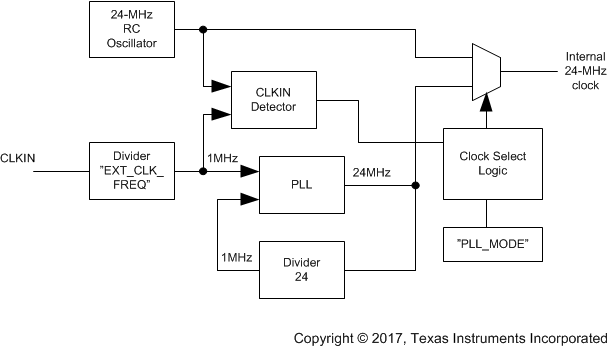
The LP8752x-Q1 device contains a CLKIN input to synchronize the switching clock of the buck regulator with the external clock. The block diagram of the clocking and PLL module is shown in Figure 13. Depending on the PLL_MODE[1:0] bits (in PLL_CTRL register) and the external clock availability, the external clock is selected, and interrupt is generated, as shown in Table 2. The interrupt can be masked with SYNC_CLK_MASK bit in TOP_MASK1 register. The nominal frequency of the external input clock is set by EXT_CLK_FREQ[4:0] bits (in PLL_CTRL register), and it can be from 1 MHz to 24 MHz with 1-MHz steps. The external clock must be inside accuracy limits (–30%/+10%) for valid clock detection.
The NO_SYNC_CLK interrupt (in INT_TOP1 register) is also generated in cases when the external clock is expected but it is not available. These cases are start-up (read OTP-to-STANDBY transition) when PLL_MODE[1:0] = 01 and regulator enable (STANDBY-to-ACTIVE transition) when PLL_MODE[1:0] = 10.
 Figure 13. Clock and PLL Module
 Table 2. PLL Operation
| DEVICE OPERATION MODE | PLL_MODE[1:0] | PLL AND CLOCK DETECTOR STATE | INTERRUPT FOR EXTERNAL CLOCK | CLOCK |
|---|---|---|---|---|
| STANDBY | 0h | Disabled | No | Internal RC |
| ACTIVE | 0h | Disabled | No | Internal RC |
| STANDBY | 1h | Enabled | When external clock appears or disappears | Automatic change to external clock when available |
| ACTIVE | 1h | Enabled | When external clock appears or disappears | Automatic change to external clock when available |
| STANDBY | 2h | Disabled | No | Internal RC |
| ACTIVE | 2h | Enabled | When external clock appears or disappears | Automatic change to external clock when available |
| STANDBY | 3h | Reserved | ||
| ACTIVE | 3h | Reserved | ||