LP8754 Multi-Phase Six-Core Step-Down Converter
1 Features
- Six High-Efficiency Step-Down DC/DC Converter Cores:
- Max Output Current 10 A
- Cores Bundled to a 6-Phase Converter
- Load Current Reporting
- Programmable Overcurrent Protection (OCP)
- Auto PWM/PFM and Forced-PWM Operations and Automatic Low Power-Mode Setting
- Automatic Phase Adding/Shedding
- Remote Differential Feedback Voltage Sensing
- Output Voltage Ramp Control
- VOUT Range = 0.6 V to 1.67 V
- I2C-Compatible Interface which Supports Standard (100 kHz), Fast (400 kHz), and High-Speed (3.4 MHz) Modes
- Four Selectable I2C Addresses
- Interrupt Function with Programmable Masking
- Output Short-Circuit and Input Overvoltage Protection (OVP)
- Spread Spectrum and Phase Control for EMI Reduction
- Overtemperature Protection (OTP)
- Undervoltage Lock-out (UVLO)
2 Applications
- Smart Phones, eBooks and Tablets
- GSM, GPRS, EDGE, LTE, CDMA and WCDMA Handsets
- Gaming Devices
3 Description
The LP8754 is designed to meet the power management requirements of the latest applications processors in mobile phones and similar portable applications. The device contains six step-down DC/DC converter cores, which are bundled together in a 6-phase buck converter. The device is fully controlled by a Dynamic Voltage Scaling (DVS) interface or an I2C-compatible serial interface.
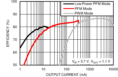
The automatic PWM/PFM operation together with the automatic phase adding/shedding maximizes efficiency over a wide output current range. The LP8754 supports remote differential voltage sensing to compensate IR drop between the regulator output and the point-of-load thus improving the accuracy of the output voltage.
The protection features include short-circuit protection, current limits, input OVP, UVLO, temperature warning, and shutdown functions. Several error flags are provided for status information of the IC. In addition, I2C read-back includes total load current and load current for each buck core: The LP8754 has the ability to sense current being delivered to the load without the addition of current sense resistors. During start-up, the device controls the output voltage slew rate to minimize overshoot and the inrush current.
Device Information(1)
| PART NUMBER | PACKAGE | BODY SIZE (MAX) |
|---|---|---|
| LP8754 | DSBGA (49) | 3.022 mm x 2.882 mm |
- For all available packages, see the orderable addendum at the end of the datasheet.
Efficiency vs. Load Current
4 Revision History
| DATE | REVISION | NOTES |
|---|---|---|
| August 2014 | Rev. A | Initial release to Web |
5 Pin Configuration and Functions
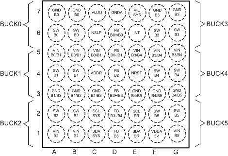
Pin Functions
| PIN | TYPE | DESCRIPTION | |
|---|---|---|---|
| NUMBER | NAME | ||
| A1, B1 | VINB2 | P | Input for Buck 2. The separate power pins VINBXX are not connected together internally - VINBXX pins must be connected together in the application and be locally bypassed. |
| A2, B2 | SWB2 | A | Buck 2 switch node |
| A3, B3, C3 | GNDB1/B2 | G | Power Ground for Buck 1 and Buck 2 |
| A4, B4 | SWB1 | A | Buck 1 switch node |
| A5, B5, C5 | VINB0/B1 | P | Input for Buck 0 and Buck 1. The separate power pins VINBXX are not connected together internally - VINBXX pins must be connected together in the application and be locally bypassed. |
| A6, B6 | SWB0 | A | Buck 0 switch node |
| A7, B7 | GNDB0 | G | Power Ground for Buck 0 |
| C1 | SDASYS | D/I/O | Serial interface data input and output for system access. Connect a pull-up resistor. |
| C2 | SCLSYS | D/I | Serial interface clock input for system access. Connect a pull-up resistor. |
| C4 | ADDR | D/I | Serial bus address selection. Connect to GND (addr = 60h), VIOSYS (addr = 61h), SDASYS (addr = 62h) or SCLSYS (addr = 63h). |
| C6 | NSLP | D/I | Full Power to Low Power state transition control signal (By default active LOW for Low-Power PFM mode) |
| C7 | VLDO | A | Internal supply voltage capacitor pin. A ceramic low ESR 1-µF capacitor should be connected from this pin to GNDA. The LDO voltage is generated internally, do NOT supply or load this pin externally. |
| D1 | FBB5 | A | Not used for six-phase converter. Connect to GND. |
| D2 | FBB3−/B4 | A | Not used for six-phase converter. Connect to GND. |
| D3 | FBB3+/B3 | A | Not used for six-phase converter. Connect to GND. |
| D4 | FBB2 | A | Not used for six-phase converter. Connect to GND. |
| D5 | FBB0−/B1 | A | Remote sensing (negative). Connect to the respective sense pin of the processor or to the negative power supply trace of the processor as close as possible to the processor. |
| D6 | FBB0+/B0 | A | Remote sensing (positive). Connect to the respective sense pin of the processor or to the positive power supply trace of the processor as close as possible to the processor. |
| D7 | GNDA | G | Ground |
| E1 | SDASR | D/I/O | Serial Interface data input and output for Dynamic Voltage Scaling (DVS). Connect a pull-up resistor / connect to GND if not used. |
| E2 | SCLSR | D/I | Serial Interface clock input for Dynamic Voltage Scaling (DVS). Connect a pull-up resistor / connect to GND if not used. |
| E3, F3, G3 | GNDB4/B5 | G | Power Ground for Buck 4 and Buck 5 |
| E4 | NRST | A | Voltage reference input for Dynamic Voltage Scaling (DVS) interface. Setting NRST input HIGH triggers start-up sequence. |
| E5, F5, G5 | VINB3/B4 | P | Input for Buck 3 and Buck 4.The separate power pins VINBXX are not connected together internally - VINBXX pins must be connected together in the application and be locally bypassed. |
| E6 | INT | D/O | Open-drain interrupt output. Active LOW. Connect a pull-up resistor to I/O supply. |
| E7 | VIOSYS | A | This pin shall be tied to the system I/O-voltage. Bias supply voltage for the device. Enables the I/O interface: All registers are accessible via serial bus interface when this pin is pulled high. An internal power-on reset (POR) occurs when VIOSYS is toggled low/high. The I2C host should allow at least 500 µs before sending data to the LP8754 after the rising edge of the VIOSYS line. |
| F1 | VDDA5V | P | Input for Analog blocks |
| F2, G2 | SWB5 | A | Buck 5 switch node |
| F4, G4 | SWB4 | A | Buck 4 switch node |
| F6, G6 | SWB3 | A | Buck 3 switch node |
| F7, G7 | GNDB3 | G | Power Ground for Buck 3 |
| G1 | VINB5 | P | Input for Buck 5. The separate power pins VINBXX are not connected together internally - VINBXX pins must be connected together in the application and be locally bypassed. |
| A: Analog Pin, D: Digital Pin, G: Ground Pin, P: Power Pin, I: Input Pin, O: Output Pin | |||