JAJSLM6 March   2021 LP87702

PRODUCTION DATA  

  1. 特長
  2. アプリケーション
  3. 概要
  4. Revision History
  5. Pin Configuration and Functions
  6. Specifications
    1. 6.1 Absolute Maximum Ratings
    2. 6.2 ESD Ratings
    3. 6.3 Recommended Operating Conditions
    4. 6.4 Thermal Information
    5. 6.5 Electrical Characteristics
    6. 6.6 I2C Serial Bus Timing Parameters
    7. 6.7 Typical Characteristics
  7. Detailed Description
    1. 7.1 Overview
    2. 7.2 Functional Block Diagram
    3. 7.3 Feature Descriptions
      1. 7.3.1  Step-Down DC/DC Converters
        1. 7.3.1.1 Overview
        2. 7.3.1.2 Transition Between PWM and PFM Modes
        3. 7.3.1.3 Buck Converter Load Current Measurement
      2. 7.3.2  Boost Converter
      3. 7.3.3  Spread-Spectrum Mode
      4. 7.3.4  Sync Clock Functionality
      5. 7.3.5  Power-Up
      6. 7.3.6  Buck and Boost Control
        1. 7.3.6.1 Enabling and Disabling Converters
        2. 7.3.6.2 Changing Buck Output Voltage
      7. 7.3.7  Enable and Disable Sequences
      8. 7.3.8  Window Watchdog
      9. 7.3.9  Device Reset Scenarios
      10. 7.3.10 Diagnostics and Protection Features
        1. 7.3.10.1 Voltage Monitorings
        2. 7.3.10.2 Interrupts
        3. 7.3.10.3 Power-Good Information to Interrupt, PG0, and PG1 Pins
          1. 7.3.10.3.1 PGx Pin Gated (Unusual) Mode
          2. 7.3.10.3.2 PGx Pin Operation in Continuous Mode
          3. 7.3.10.3.3 Summary of PG0, PG1 Gated, and Continuous Operating Modes
        4. 7.3.10.4 Warning Interrupts for System Level Diagnostics
          1. 7.3.10.4.1 Output Power Limit
          2. 7.3.10.4.2 Thermal Warning
        5. 7.3.10.5 Protections Causing Converter Disable
          1. 7.3.10.5.1 Short-Circuit and Overload Protection
          2. 7.3.10.5.2 Overvoltage Protection
          3. 7.3.10.5.3 Thermal Shutdown
        6. 7.3.10.6 Protections Causing Device Power Down
          1. 7.3.10.6.1 Undervoltage Lockout
      11. 7.3.11 OTP Error Correction
      12. 7.3.12 Operation of GPO Signals
      13. 7.3.13 Digital Signal Filtering
    4. 7.4 Device Functional Modes
      1. 7.4.1 Modes of Operation
    5. 7.5 Programming
      1. 7.5.1 I2C-Compatible Interface
        1. 7.5.1.1 Data Validity
        2. 7.5.1.2 Start and Stop Conditions
        3. 7.5.1.3 Transferring Data
        4. 7.5.1.4 I2C-Compatible Chip Address
        5. 7.5.1.5 Auto Increment Feature
    6. 7.6 Register Maps
      1. 7.6.1 Register Descriptions
        1. 7.6.1.1 LP8770_map Registers
  8. Application and Implementation
    1. 8.1 Application Information
    2. 8.2 Typical Application
      1. 8.2.1 Design Requirements
      2. 8.2.2 Detailed Design Procedure
        1. 8.2.2.1 Application Components
          1. 8.2.2.1.1 Inductor Selection
          2. 8.2.2.1.2 Buck Input Capacitor Selection
          3. 8.2.2.1.3 Buck Output Capacitor Selection
          4. 8.2.2.1.4 Boost Input Capacitor Selection
          5. 8.2.2.1.5 Boost Output Capacitor Selection
          6. 8.2.2.1.6 Supply Filtering Components
      3. 8.2.3 Current Limit vs Maximum Output Current
      4. 8.2.4 Application Curves
  9. Power Supply Recommendations
  10. 10Layout
    1. 10.1 Layout Guidelines
    2. 10.2 Layout Example
  11. 11Device and Documentation Support
    1. 11.1 Third-Party Products Disclaimer
    2. 11.2 Receiving Notification of Documentation Updates
    3. 11.3 サポート・リソース
    4. 11.4 Trademarks
    5. 11.5 静電気放電に関する注意事項
    6. 11.6 用語集
  12. 12Mechanical, Packaging, and Orderable Information

パッケージ・オプション

メカニカル・データ(パッケージ|ピン)
サーマルパッド・メカニカル・データ
発注情報

Sync Clock Functionality

The LP87702 device contains a CLKIN input to synchronize buck and boost converters' switching clock with the external clock. Figure 7-3 shows the block diagram of the clocking and PLL module. Table 7-2 shows how the external clock is selected and interrupt is generated depending on the EN_PLL bit in PLL_CTRL register and the external clock availability. The interrupt can be masked with SYNC_CLK_MASK bit in TOP_MASK_1 register. The nominal frequency of the external input clock is set by EXT_CLK_FREQ[4:0] bits in PLL_CTRL register and it can be from 1 MHz to 24 MHz with 1-MHz steps. The external clock must be inside accuracy limits (–30%/+10%) for valid clock detection.

The SYNC_CLK_INT interrupt in INT_TOP_1 register is also generated in cases the external clock is expected but it is not available. These cases are Startup (Read OTP-to-standby transition) when EN_PLL = 1 and buck or boost converter is enabled (standby-to-active transition) when EN_PLL = 1.
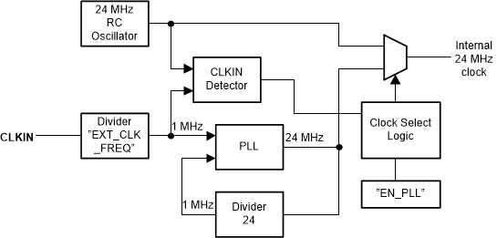
GUID-07C81734-AD66-49CD-BBBA-C0C6D934527A-low.gifFigure 7-3 Clock and PLL Module
Table 7-2 PLL Operation
DEVICE OPERATION MODEEN_PLLPLL AND CLOCK DETECTOR STATEINTERRUPT FOR EXTERNAL CLOCKCLOCK
STANDBY0DisabledNoInternal RC
ACTIVE0DisabledNoInternal RC
STANDBY1EnabledWhen external clock disappears or appearsAutomatic change to internal RC oscillator when External clock is not available
ACTIVE1EnabledWhen external clock disappears or appearsAutomatic change to internal RC oscillator when External clock is not available