JAJSCD8C August 2015 – May 2017 LP8861-Q1
PRODUCTION DATA.
- 1 特長
- 2 アプリケーション
- 3 概要
- 4 改訂履歴
- 5 デバイス比較表
- 6 Pin Configuration and Functions
-
7 Specifications
- 7.1 Absolute Maximum Ratings
- 7.2 ESD Ratings
- 7.3 Recommended Operating Conditions
- 7.4 Thermal Information
- 7.5 Electrical Characteristics
- 7.6 Internal LDO Electrical Characteristics
- 7.7 Protection Electrical Characteristics
- 7.8 Power Line FET Control Electrical Characteristics
- 7.9 Current Sinks Electrical Characteristics
- 7.10 PWM Brightness Control Electrical Characteristics
- 7.11 Boost/SEPIC Converter Characteristics
- 7.12 Logic Interface Characteristics
- 7.13 Typical Characteristics
-
8 Detailed Description
- 8.1 Overview
- 8.2 Functional Block Diagram
- 8.3 Feature Description
- 8.4 Device Functional Modes
-
9 Application and Implementation
- 9.1 Application Information
- 9.2 Typical Applications
- 10Power Supply Recommendations
- 11Layout
- 12デバイスおよびドキュメントのサポート
- 13メカニカル、パッケージ、および注文情報
パッケージ・オプション
メカニカル・データ(パッケージ|ピン)
- PWP|20
サーマルパッド・メカニカル・データ
- PWP|20
発注情報
8.3.6.2 Overview of the Fault/Protection Schemes
The LP8861-Q1 fault detection behavior is described in Table 3. Detected faults (excluding LED faults) cause the device to enter FAULT_RECOVERY state. In FAULT_RECOVERY the boost and LED outputs of LP8861-Q1 are disabled, power-line FET is turned off, and the FAULT pin is pulled low. Device recovers automatically and enters normal operating mode (ACTIVE) after a recovery time of 100 ms if the fault condition has disappeared. When recovery is successful, the FAULT pin is released.
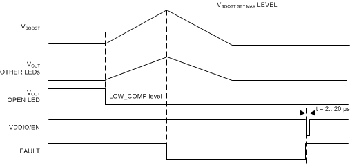
In case a LED fault is detected, device continues normal operation and only the faulty string is disabled. Fault is indicated via FAULT pin which can be released by toggling VDDIO/EN pin low for a short period of 2…20 µs. LEDs are turned off for this period but device stays in ACTIVE mode. If VDDIO/EN is low longer, device goes to STANDBY and restarts when EN goes high again.
Table 3. Fault/Protection Schemes
| FAULT/
PROTECTION |
FAULT NAME | THRESHOLD | CONNECTED TO
FAULT PIN |
FAULT_
RECOVERY STATE |
ACTION |
|---|---|---|---|---|---|
| VIN overvoltage protection | VIN_OVP | 1. VIN > 42 V
2. VBOOST > VSET_BOOST + (6...10) V VSET_BOOST is voltage value defined by logic during adaptation |
Yes | Yes | 1. Overvoltage is monitored from the beginning of soft start. Fault is detected if the duration of overvoltage condition is 100 µs minimum.
2. Overvoltage is monitored from the beginning of normal operation (ACTIVE mode). Fault is detected if overvoltage condition duration is 560 ms minimum (tfilter). After the first fault detection filter time is reduced to 50 ms for following recovery cycles. When device recovers and has been in ACTIVE mode for 160 ms, filter is increased back to 560 ms. |
| VIN undervoltage lockout | VIN_UVLO | Falling 3.9 V
Rising 4 V |
Yes | Yes | Detects undervoltage condition at VIN pin. Sensed from the beginning of soft start. Fault is detected if undervoltage condition duration is 100 µs minimum. |
| VIN overcurrent protection | VIN_OCP | 3 A (50-mΩ current sensor resistor) | Yes | Yes | Detects overcurrent by measuring voltage of the SENSE resistor connected between VIN and VSENSE_N pins. Sensed from the beginning of soft start. Fault is detected if undervoltage condition duration is 10 µs minimum. |
| Open LED fault | OPEN_LED | LOW_COMP threshold | Yes | No | Detected if one or more outputs are below threshold level, and boost adaptive control has reached maximum voltage. Open string(s) is removed from voltage control loop and PWM is disabled.
Fault pin is cleaned by toggling VDDIO/EN pin. If VDDIO/EN is low for a short period of 2…20 µs, LEDs are turned off for this period but device stays ACTIVE. If VDDIO/EN is low longer, device goes to STANDBY and restarts when EN goes high again. |
| Shorted LED fault | SHORT_LED | Shorted string detection level 6 V | Yes | No | Detected if one or more outputs voltages are above shorted string detection level and at least one LED output voltage is within headroom window. Shorted string(s) are removed from the boost voltage control loop and outputs PWM(s) are disabled.
Fault pin is cleaned by toggling VDDIO/EN pin. If VDDIO/EN is low for a short period of 2…20 µs, LEDs are turned off for this period but device stays ACTIVE. If VDDIO/EN is low longer, device goes to STANDBY and restarts when EN goes high again. |
| Thermal protection | TSD | 165ºC
Thermal Shutdown Hysteresis 20ºC |
Yes | Yes | Thermal shutdown is monitored from the beginning of soft start. Die temperature must decrease by 20ºC for device to recover. |
 Figure 16. VIN Overvoltage Protection (Boost OVP)
  Figure 17. VIN Overvoltage Protection (VIN OVP)
  Figure 18. VIN Undervoltage Lockout
  Figure 19. Input Voltage Overcurrent Protection
  Figure 20. LED Open Fault
  Figure 21. LED Short Fault